

Method for operating flash memory and system chip
A system chip and non-volatile storage technology, which is applied to a method of operating flash memory and the field of system chips, can solve problems such as component compatibility problems, and achieve the effect of overcoming incompatibility
- Summary
- Abstract
- Description
- Claims
- Application Information
AI Technical Summary
Problems solved by technology
Method used
Image

Examples
Embodiment Construction
[0022] In order to make the technical problems, technical solutions and advantages to be solved by the present invention clearer, the following will describe in detail with reference to the drawings and specific embodiments.
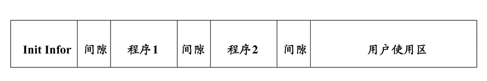
[0023] Firmware (firmware), as the bootloader of the system chip, is a small program that runs before the operating system kernel runs, initializes hardware devices, and establishes a memory space map, thereby setting the software and hardware environment of the system in a suitable state for the final call The operating system kernel prepares the correct environment. In the present invention, the execution path of the firmware is changed without changing the firmware.
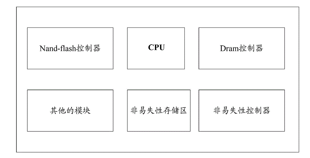
[0024] SoC such as image 3 As shown, including: non-volatile controller, non-volatile storage area, Nand-flash controller, CPU, Dram controller and other modules, where the non-volatile controller is used to read the non-volatile data in permanent storage.
[0025] An embodiment of t...
PUM
 Abstract
Description
Claims
Application Information