

An Electron Beam Exposure Method Using Ultraviolet Curing Glue
A technology of electron beam exposure and electron beam lithography, which is applied to the processing of circuits, electrical components, photosensitive materials, etc., can solve the problems of incompatibility of developing process and limit the application range of LOL, so as to reduce the corrosion of developing solution and improve the cross-sectional shape appearance, contrast-enhancing effects
- Summary
- Abstract
- Description
- Claims
- Application Information
AI Technical Summary
Problems solved by technology
Method used
Image

Examples
Embodiment 1
[0036] 1. Clean the substrate and apply the HMDS adhesive layer.
[0037] The material of the substrate in this embodiment is Si. Using a vacuum oven, gaseously adsorb the HMDS adhesive layer on the substrate. The temperature of the vacuum oven is 180°C, and the time is 40s.
[0038] 2. Spin-coat the lift-off layer photoresist LOL with a thickness of 40nm.
[0039] The thickness of LOL will affect the undercutting and graphics accuracy, the determination of the thickness is related to the line width requirement, the smaller the line width, the thinner the LOL.
[0040] 3. Substrate baking (baking before peeling off the layer).
[0041] The role of baking is to remove the residual solvent in the film. It is a standard process provided by photoresist manufacturers and is carried out according to the recommended conditions of LOL. The recommended condition of LOL in this embodiment refers to 170° C., using a hot plate to bake for 5 minutes.
[0042] 4. Spin-coat negative ele...
Embodiment 2
[0056] 1. Clean the substrate and apply the HMDS adhesive layer.
[0057] The material of the substrate in this embodiment is Si. Spin-coat liquid HMDS with a homogenizer at 3000rpm for 10s, then bake with a hot plate under the following conditions: temperature 98°C, time 5min
[0058] 2. Spin-coat the lift-off layer photoresist LOL with a thickness of 40nm.
[0059] 3. Substrate baking (baking before peeling off the layer).
[0060] The recommended conditions of LOL in this embodiment refer to 150°C, and bake in an oven for 40 minutes.
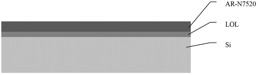
[0061] 4. Spin-coat negative electron beam photoresist AR-N7520 with a thickness of 150nm.
[0062] figure 1 It is a schematic diagram after spin-coating two-layer photoresist AR-N7520 / LOL.
[0063] 5. Substrate baking (beam photoresist pre-baking).
[0064] According to the recommended conditions of AR-N7520. Here, the recommended conditions for AR-N7520 are 75°C, baked in an oven for 35 minutes.
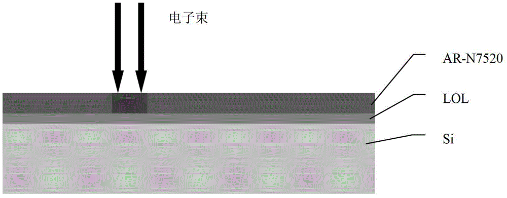
[0065] 6. Electron beam exposure (p...
PUM
| Property | Measurement | Unit |
|---|---|---|
| wavelength | aaaaa | aaaaa |
Abstract
Description
Claims
Application Information