Minitype LED array chip

A LED array and chip technology, which is applied in the direction of electrical components, circuits, semiconductor devices, etc., can solve the problems such as the difficulty of making the size of the light-emitting unit small, the inability to meet the needs, and the limitation of resolution, so as to achieve the effect of light-emitting display

Active Publication Date: 2013-11-20
CHANGCHUN INST OF OPTICS FINE MECHANICS & PHYSICS CHINESE ACAD OF SCI
View PDF5 Cites 14 Cited by
  • Summary
  • Abstract
  • Description
  • Claims
  • Application Information

AI Technical Summary

Problems solved by technology

[0003] The present invention provides a miniature LED array chip to solve the problem that the size of the light-emitting unit of the LED in the existing LED microdisplay is difficult to be made small, resulting in limited resolution and inability to meet the needs.

Method used


Image

  • Minitype LED array chip
  • Minitype LED array chip
  • Minitype LED array chip

Examples


specific Embodiment approach 1

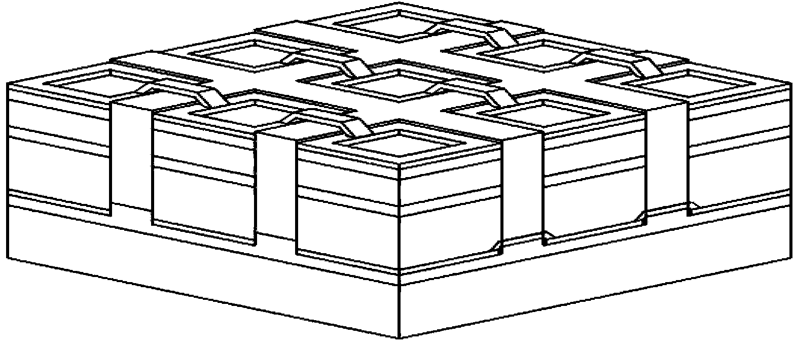
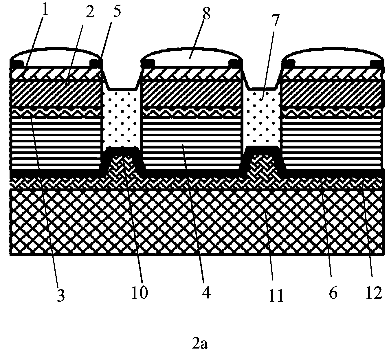
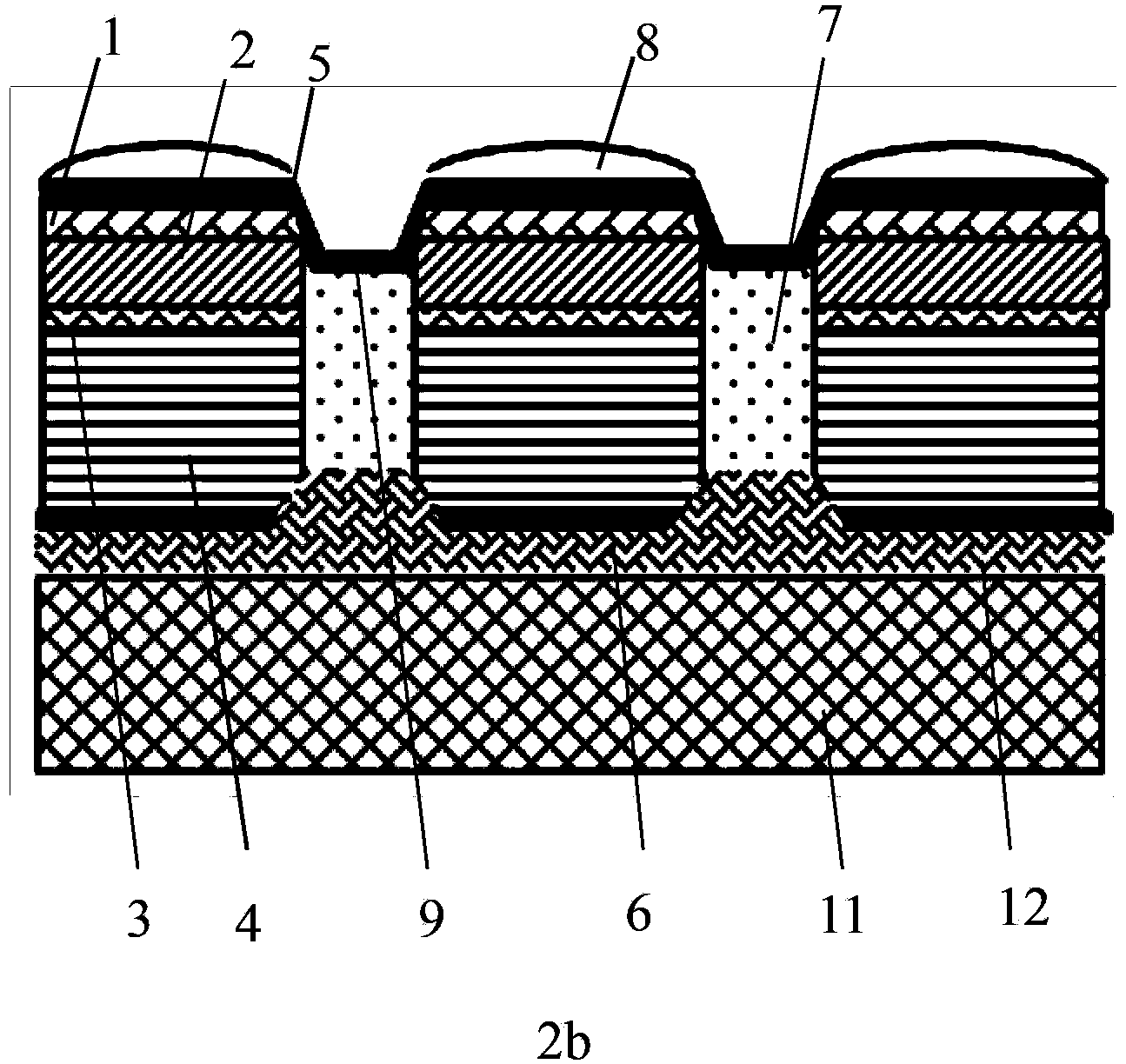
[0015] Specific implementation mode 1. Combination Figure 1 to Figure 8 Describe this embodiment mode, a micro-LED array chip, including a light-transmitting layer 1, a light-emitting layer 2, a reflective layer 3, a substrate 4, an upper electrode 5, an upper electrode lead 9, a lower electrode 6, a lower electrode lead 10, and a diaphragm 7. Microlens 8 and substrate 11;

[0016] The light-transmitting layer 1, light-emitting layer 2, reflective layer 3, substrate 4 and micro-lens 8 form a square or rectangular or circular or other shaped LED light emitting unit. The upper surface of the reflective layer 3 is the luminous layer 2 , the light-transmissive layer 1 and the microlens 8 in sequence, and the lower surface of the reflective layer 3 is the substrate 4 . The LED light-emitting units are uniformly arranged to form a light-emitting unit array. Between the light-emitting units is an aperture 7, which connects each light-emitting unit in sequence and realizes the isol...


PUM


Abstract

The invention discloses a minitype LED array chip, which relates to the technical field of LED, and solves the problems existing in a conventional manufactured LED micro display that the sizes of lighting units are hard to be small, the resolution ratio is caused to be limited, and the requirements cannot be adapted. The working process of the minitype LED array chip is as follows: current is injected from upper electrodes and flows out from lower electrodes, and an electric field is formed in a device to allow current carriers to illuminate in recombination in luminous layers. According to the invention, partial light passes through euphotic layers upwards, and is irradiated out through micro lenses, and partial light reaches to reflecting layers downwards, is reflected by the reflecting layers, and is irradiated from the micro lenses after penetrating the luminous layers and euphotic layers. As the lighting principle of an illuminator is illuminating in recombination of the current carriers a p-n junction; the principle has the nonlinear propertys of current and voltage of a diode; the luminance has the nonlinear property with the size of the injection current. The chip controls the luminance of pixel elements through a circuit to realize the luminous display.

Description

technical field [0001] The invention relates to the technical field of LEDs, in particular to an LED integrated chip. Background technique [0002] At present, micro-display devices have become the focus of attention of all scientific and technological powers by virtue of their unique advantages. LED microdisplays have many unique advantages, such as active light emission, ultra-high brightness, long life, low operating voltage, high luminous efficiency, fast response, stable and reliable performance, and wide operating temperature range. The traditional manufacturing method is to arrange multiple single-tube LED chips on the base, and then wire and package. Affected by the base, it is difficult to reduce the size of the light-emitting unit of the display device manufactured by this method, so the resolution is limited to a certain extent, and it does not meet the development needs of miniaturization and clarity in the future. Combining semiconductor process technology wit...

Claims


Application Information

Patent Timeline
IPC IPC(8): H01L33/36H01L33/38H01L33/40H01L33/58
Inventor 梁静秋梁中翥王维彪田超秦余欣吕金光包兴臻
Owner CHANGCHUN INST OF OPTICS FINE MECHANICS & PHYSICS CHINESE ACAD OF SCI
Why Eureka
Try Eureka