
Miniature flexible LED area array device with high luminous uniformity and preparation method

A uniform and miniature technology, applied in the field of light-emitting display, can solve the problems of limited application range, luminous brightness, uniform luminous efficiency not as good as LED, limiting the application and development of OLED, etc., to achieve uniform current distribution, simple and easy manufacturing process, The effect of high luminous efficiency

Active Publication Date: 2016-03-02
CHANGCHUN INST OF OPTICS FINE MECHANICS & PHYSICS CHINESE ACAD OF SCI
View PDF3 Cites 0 Cited by
  • Summary
  • Abstract
  • Description
  • Claims
  • Application Information

AI Technical Summary

Problems solved by technology

Compared with traditional light-emitting devices, planar LED microdisplay arrays have many incomparable advantages, but their application range is largely limited due to their inflexibility.
Although OLED technology has a good application prospect, compared with LED, there are still some shortcomings. For example, there are still some problems in micro-miniature devices, such as luminous brightness, uniformity, luminous efficiency, etc. are not as good as LED, and the most prominent is Lifespan problems, these problems will greatly limit the application and development of OLED

Method used


Image

  • Miniature flexible LED area array device with high luminous uniformity and preparation method
  • Miniature flexible LED area array device with high luminous uniformity and preparation method
  • Miniature flexible LED area array device with high luminous uniformity and preparation method

Examples


specific Embodiment approach 1

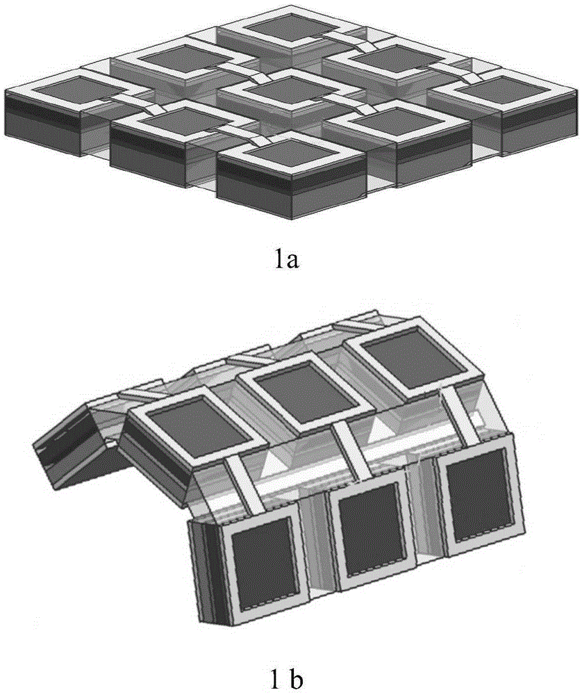
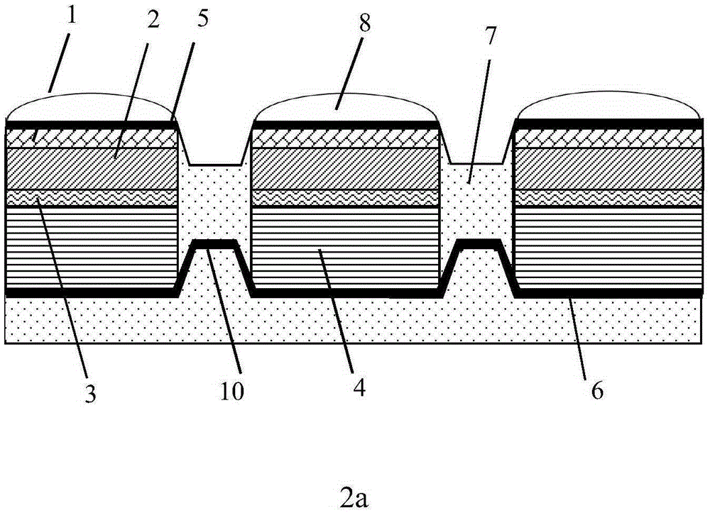
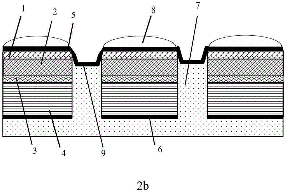
[0033] Specific implementation mode 1. Combination Figure 1 to Figure 8 To illustrate this embodiment, the highly uniform micro-flexible LED area array device described in this embodiment includes: a light-transmitting layer 1, a light-emitting layer 2, a reflective layer 3, a substrate 4, an upper electrode 5, an upper electrode lead 9, a lower Electrode 6, lower electrode lead 10, flexible region 7 and microlens 8; the top of reflective layer 3 is light-emitting layer 2, light-transmitting layer 1, upper electrode 5 and microlens 8, and the bottom of reflective layer 3 is substrate 4. The light-transmitting layer 1, the light-emitting layer 2, the reflective layer 3 and the substrate 4 form an LED light-emitting unit. The LED light-emitting units are uniformly arranged to form a light-emitting unit array. There is a flexible area 7 between the light emitting units, and the flexible area 7 connects each light emitting unit sequentially and makes the entire LED light emittin...

specific Embodiment approach 2

[0036] Specific embodiment two, combine Figure 9 with Figure 10 To illustrate this embodiment, the highly uniform miniature flexible LED area array device described in this embodiment adopts a top-down manufacturing method, first fabricating the front structure, and then protecting the front structure to prepare the back structure. The specific process is:

[0037] A. Cleaning and front protection of light-emitting chips:

[0038] a) The host material used in the present invention is a light-emitting chip, and the light-emitting chip used is composed of a light-transmitting layer, a light-emitting layer, a reflective layer and a substrate, such as Figure 9 as shown in a.

[0039] b) Cleaning the light-emitting chip. Then prepare a layer of protective film on the upper surface of the light-emitting chip, that is, the upper surface of the light-transmitting layer, such as Figure 9 as shown in b.

[0040] B. Preparation of upper isolation trench:

[0041] Through photo...

specific Embodiment approach 3

[0065] Specific implementation mode three. This implementation mode is an example of the preparation method of the highly uniform miniature flexible LED area array device described in the specific implementation mode two: the specific method is:

[0066] A. Cleaning and front protection of light-emitting chips:

[0067] a) The light-emitting chip used in the present invention is an AlGaInP-LED epitaxial wafer, which is composed of a light-transmitting layer, a light-emitting layer, a reflective layer and a substrate, and the thickness of the light-emitting chip is 200 μm to 1000 μm.

[0068] b) The material of the upper protective film is silicon dioxide or silicon nitride or a composite film composed of silicon dioxide and silicon nitride or metal or organic material or inorganic material or other film materials that can play a protective role. The preparation method of the protective film is electron beam evaporation, radio frequency sputtering, magnetron sputtering, sol-gel...


PUM


Abstract

The invention discloses a high-luminescence-uniformity miniaturized flexible LED area array device and a preparation method thereof, and relates to the field of luminescence display technologies. With the device and method, the problem of limited use due to bending incapability of a conventional planar LED micro-display device can be solved. Current is injected from a graphene transparent upper electrode and flows out of a lower electrode, so that an electric field is formed in the device, and positive and negative carriers emit light at a luminescent layer in a composite manner; a part of the light is oriented upwards, passes through an euphotic layer and the graphene transparent upper electrode and comes out of a micro-lens; and a part of the light is oriented downwards, reaches a reflection layer, is reflected by the reflection layer, passes through the luminescent layer, the euphotic layer and the graphene transparent upper electrode, and then comes out of the micro-lens. The luminescent device is based on the luminescence principle of composite luminescence of the carriers in a p-n structure and has the non-linear characteristics of the current and voltage of a diode so that the luminescent brightness also has the non-linear characteristics according to the size of the injected current. The brightness of pixel elements is controlled through a circuit so that luminescence display is realized.

Description

technical field [0001] The invention belongs to the technical field of light emitting display, and relates to a novel micro flexible light emitting device, in particular to an AlGaInP-LED flexible micro device and a manufacturing method. Background technique [0002] In recent years, with the development of the electronic industry, micro light emitting devices have developed rapidly. Compared with traditional light-emitting devices, planar LED microdisplay arrays have many incomparable advantages, but their application range is largely limited due to their inflexibility. Although OLED technology has good application prospects, compared with LED, there are still some shortcomings. For example, there are still some problems in micro-miniature devices, such as luminous brightness, uniformity, and luminous efficiency. Lifespan issues, these issues will limit the application and development of OLED to a large extent. With the development of science and technology, there is an i...

Claims


Application Information

Patent Timeline
Patent Type & Authority Patents(China)
IPC IPC(8): H01L25/13H01L33/38H01L33/42H01L33/00
Inventor 梁静秋梁中翥王维彪田超秦余欣吕金光
Owner CHANGCHUN INST OF OPTICS FINE MECHANICS & PHYSICS CHINESE ACAD OF SCI
Learn More