Semiconductor device, display device including the semiconductor device, display module including the display device, and electronic device including the semiconductor device, the display device, and the display module

a technology of semiconductor devices and semiconductor devices, applied in the direction of semiconductor devices, electrical devices, transistors, etc., can solve the problems of inability to store written to the pixel, image quality degradation of the display device, and large occupation area of the inverted staggered transistor, etc., to achieve low manufacturing cost, signal delay, and relatively simple manufacturing process

Active Publication Date: 2015-08-06
SEMICON ENERGY LAB CO LTD
View PDF1 Cites 175 Cited by
  • Summary
  • Abstract
  • Description
  • Claims
  • Application Information

AI Technical Summary

Benefits of technology

[0010]As a transistor including an oxide semiconductor film, an inverted staggered transistor (also referred to as a transistor having a bottom-gate structure), a planar transistor (also referred to as a transistor having a top-gate structure), and the like are given. In the case where a transistor including an oxide semiconductor film is used for a display device, an inverted staggered transistor is used more often than a planar transistor because a manufacturing process thereof is relatively simple and manufacturing cost thereof can be kept low. However, signal delay or the like is increased by parasitic capacitance that exists between a gate electrode and source and drain electrodes of an inverted staggered transistor and accordingly image quality of a display device degrades, which has posed a problem, as an increase in screen size of a display device proceeds, or a display device is provided with a higher resolution image (for example, a high-resolution display device typified by 4 k×2 k pixels (3840 pixels in the horizontal direction and 2160 pixels in the perpendicular direction) or 8 k×4 k pixels (7680 pixels in the horizontal direction and 4320 pixels in the perpendicular direction)). Furthermore, as another problem, the occupation area of an inverted staggered transistor is larger than that of a planar transistor. Thus, with regard to a planar transistor including an oxide semiconductor film, development of a transistor which has a structure with stable semiconductor characteristics and high reliability and which is formed by a simple manufacturing process is desired.

Problems solved by technology

However, signal delay or the like is increased by parasitic capacitance that exists between a gate electrode and source and drain electrodes of an inverted staggered transistor and accordingly image quality of a display device degrades, which has posed a problem, as an increase in screen size of a display device proceeds, or a display device is provided with a higher resolution image (for example, a high-resolution display device typified by 4 k×2 k pixels (3840 pixels in the horizontal direction and 2160 pixels in the perpendicular direction) or 8 k×4 k pixels (7680 pixels in the horizontal direction and 4320 pixels in the perpendicular direction)).
Furthermore, as another problem, the occupation area of an inverted staggered transistor is larger than that of a planar transistor.
Depending on the structure of the capacitor, there has been a problem in that data written to the pixel cannot be stored and the image quality of the display device is degraded.

Method used


Image

  • Semiconductor device, display device including the semiconductor device, display module including the display device, and electronic device including the semiconductor device, the display device, and the display module
  • Semiconductor device, display device including the semiconductor device, display module including the display device, and electronic device including the semiconductor device, the display device, and the display module
  • Semiconductor device, display device including the semiconductor device, display module including the display device, and electronic device including the semiconductor device, the display device, and the display module

Examples


embodiment 1

[0081]In this embodiment, a semiconductor device in which a transistor and a capacitor are provided over the same substrate and a method for manufacturing the semiconductor device are described with reference to FIGS. 1A to 1D, FIG. 2, FIGS. 3A to 3D, FIGS. 4A and 4B, FIGS. 5A to 5D, FIG. 6, FIGS. 7A to 7D, FIGS. 8A to 8D, FIGS. 9A to 9D, FIG. 10, FIGS. 11A to 11C, FIGS. 12A to 12H, FIGS. 13A to 13F, FIGS. 14A to 14F, FIGS. 15A to 15F, and FIGS. 16A to 16F.

1 of Semiconductor Device>

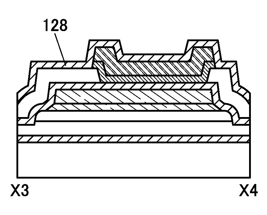
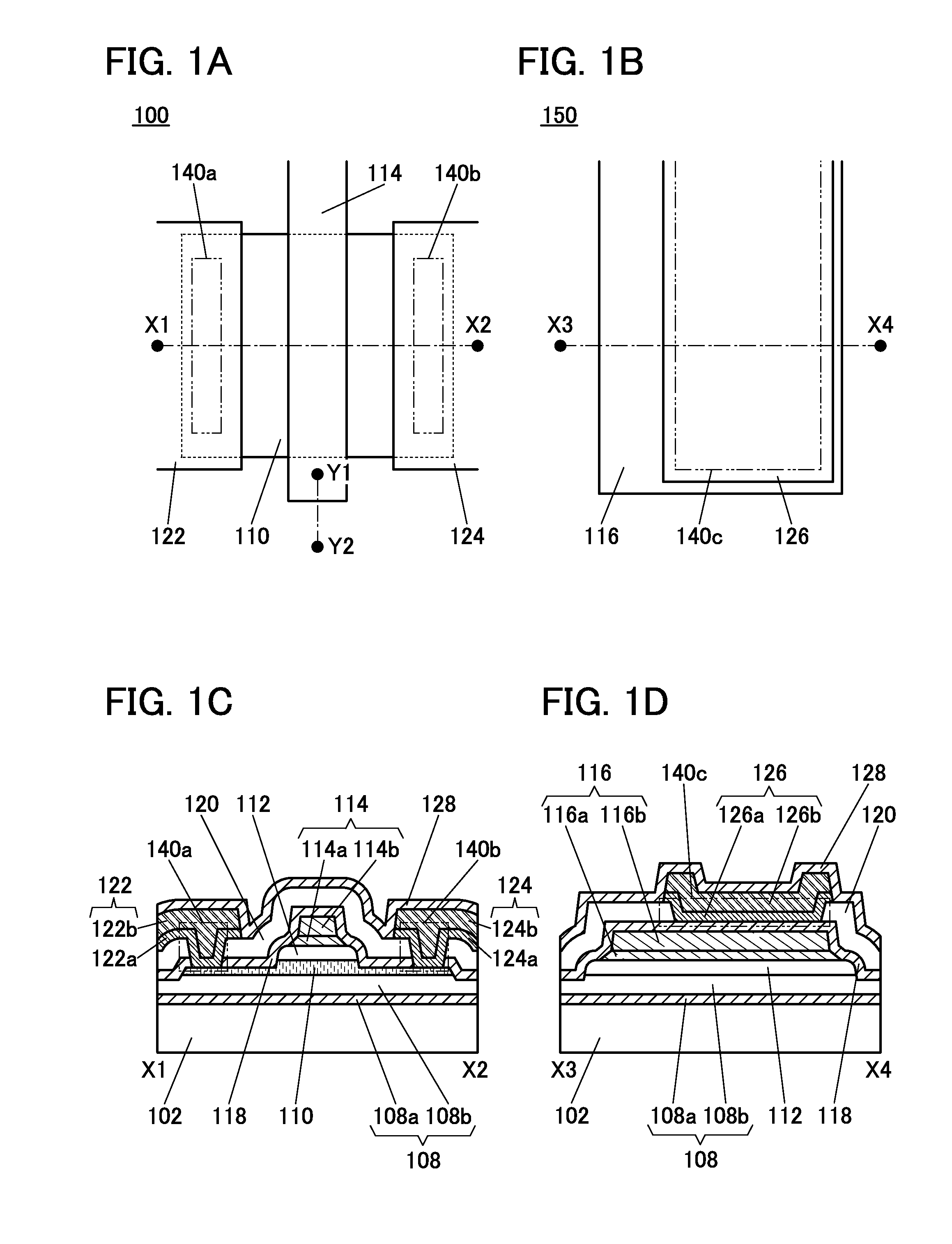
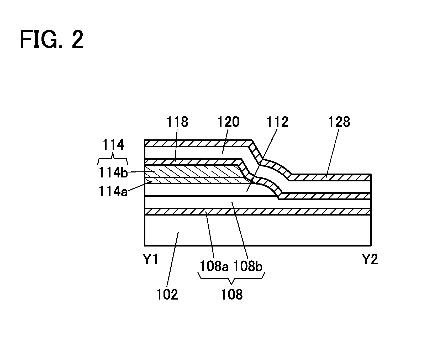
[0082]FIGS. 1A to 1D illustrate an example of a semiconductor device in which a transistor and a capacitor are provided over the same substrate. Note that the transistor has a top-gate structure.

[0083]FIG. 1A is a top view of a transistor 100 included in the semiconductor device. FIG. 1B is a top view of a capacitor 150 included in the semiconductor device. FIG. 1C is a cross-sectional view along the dashed-dotted line X1-X2 in FIG. 1A. FIG. 1D is a cross-sectional view along the dashed-dotted line X3-X4 ...

embodiment 2

[0325]In this embodiment, the structure of an oxide semiconductor film included in a semiconductor device of one embodiment of the present invention is described below in detail.

[0326]First, a structure which can be included in an oxide semiconductor film is described below.

[0327]An oxide semiconductor film is classified roughly into a single-crystal oxide semiconductor film and a non-single-crystal oxide semiconductor film. The non-single-crystal oxide semiconductor film includes any of a c-axis aligned crystalline oxide semiconductor (CAAC-OS) film, a polycrystalline oxide semiconductor film, a microcrystalline oxide semiconductor film, an amorphous oxide semiconductor film, and the like.

[0328]First, a CAAC-OS film is described.

[0329]The CAAC-OS film is one of oxide semiconductor films having a plurality of c-axis aligned crystal parts.

[0330]In a transmission electron microscope (TEM) image of the CAAC-OS film, a boundary between crystal parts, that is, a grain boundary is not cle...

embodiment 3

[0421]In this embodiment, an oxygen vacancy of an oxide semiconductor film is described in detail below.

oH>

[0422]In the case where an oxide semiconductor film (hereinafter referred to as IGZO) is a complete crystal, H preferentially diffuses along the a-b plane at a room temperature. In heat treatment at 450° C., H diffuses along the a-b plane and in the c-axis direction. Here, description is made on whether H easily enters an oxygen vacancy Vo if the oxygen vacancy Vo exists in IGZO. A state in which H is in an oxygen vacancy Vo is referred to as VoH.

[0423]An InGaZnO4 crystal model shown in FIG. 20 was used for calculation. The activation barrier (Ea) along the reaction path where H in VoH is released from Vo and bonded to oxygen was calculated by a nudged elastic band (NEB) method. The calculation conditions are shown in Table 2.

TABLE 2SoftwareVASPCalculation methodNEB methodFunctionalGGA-PBEPseudopotentialPAWCut-off energy500 eVK points2 × 2 × 3

[0424]In the InGaZnO4 crystal model...


PUM


Abstract

To provide a semiconductor device including a planar transistor having an oxide semiconductor and a capacitor. In a semiconductor device, a transistor includes an oxide semiconductor film, a gate insulating film over the oxide semiconductor film, a gate electrode over the gate insulating film, a second insulating film over the gate electrode, a third insulating film over the second insulating film, and a source and a drain electrodes over the third insulating film; the source and the drain electrodes are electrically connected to the oxide semiconductor film; a capacitor includes a first and a second conductive films and the second insulating film; the first conductive film and the gate electrode are provided over the same surface; the second conductive film and the source and the drain electrodes are provided over the same surface; and the second insulating film is provided between the first and the second conductive films.

Description

BACKGROUND OF THE INVENTION[0001]1. Field of the Invention[0002]One embodiment of the present invention relates to a semiconductor device including an oxide semiconductor film and a display device including the semiconductor device.[0003]Note that one embodiment of the present invention is not limited to the above technical field. The technical field of one embodiment of the invention disclosed in this specification and the like relates to an object, a method, or a manufacturing method. In addition, the present invention relates to a process, a machine, manufacture, or a composition of matter. In particular, one embodiment of the present invention relates to a semiconductor device, a display device, a light-emitting device, a power storage device, a storage device, a driving method thereof, or a manufacturing method thereof.[0004]In this specification and the like, a semiconductor device generally means a device that can function by utilizing semiconductor characteristics. A semicon...

Claims


Application Information

Patent Timeline
Patent Type & Authority Applications(United States)
IPC IPC(8): H01L27/12
CPCH01L27/1255H01L27/1225H01L29/7869H01L29/78696H10K59/1213H01L29/78606H10K59/805H10K59/131H01L29/78645H01L27/14609H01L27/14612H01L27/14634H10K59/1216H01L29/4908H01L29/78603H01L29/78648
Inventor YAMAZAKI, SHUNPEIOKAZAKI, KENICHIKATAYAMA, MASAHIRONAKADA, MASATAKA
Owner SEMICON ENERGY LAB CO LTD
Why Eureka
Try Eureka