Semiconductor device including an oxide semiconductor and the display device including the semiconductor device

a semiconductor and semiconductor technology, applied in the direction of transistors, electroluminescent light sources, electric lighting sources, etc., can solve the problems of large occupation area of inverted staggered transistors, image quality degradation of display devices, etc., to achieve low manufacturing cost, signal delay, and relatively simple manufacturing process

Active Publication Date: 2017-02-21
SEMICON ENERGY LAB CO LTD
View PDF143 Cites 7 Cited by
  • Summary
  • Abstract
  • Description
  • Claims
  • Application Information

AI Technical Summary

Benefits of technology

[0009]As a transistor including an oxide semiconductor film, an inverted staggered transistor (also referred to as a transistor having a bottom-gate structure), a planar transistor (also referred to as a transistor having a top-gate structure), and the like are given. In the case where a transistor including an oxide semiconductor film is used for a display device, an inverted staggered transistor is used more often than a planar transistor because a manufacturing process thereof is relatively simple and manufacturing cost thereof can be kept low. However, signal delay or the like is increased by parasitic capacitance that exists between a gate electrode and source and drain electrodes of an inverted staggered transistor and accordingly image quality of a display device degrades, which has posed a problem, as an increase in screen size of a display device proceeds, or a display device is provided with a higher resolution image (for example, a high-resolution display device typified by 4 k×2 k pixels (3840 pixels in the horizontal direction and 2048 pixels in the perpendicular direction) or 8 k×4 k pixels (7680 pixels in the horizontal direction and 4320 pixels in the perpendicular direction)). Furthermore, as another problem, the occupation area of an inverted staggered transistor is larger than that of a planar transistor. Thus, with regard to a planar transistor including an oxide semiconductor film, development of a transistor which has a structure with stable semiconductor characteristics and high reliability and which is formed by a simple manufacturing process is desired.
[0021]One embodiment of the present invention can provide a novel semiconductor device including an oxide semiconductor. In particular, a planar type semiconductor device including an oxide semiconductor can be provided. A semiconductor device including an oxide semiconductor in which on-state current is high can be provided, a semiconductor device including an oxide semiconductor in which off-state current is low can be provided, a semiconductor device including an oxide semiconductor that occupies a small area can be provided, a semiconductor device including an oxide semiconductor that has a stable electrical characteristic can be provided, a semiconductor device including an oxide semiconductor that has high reliability can be provided, a novel semiconductor device can be provided, or a novel display device can be provided.

Problems solved by technology

However, signal delay or the like is increased by parasitic capacitance that exists between a gate electrode and source and drain electrodes of an inverted staggered transistor and accordingly image quality of a display device degrades, which has posed a problem, as an increase in screen size of a display device proceeds, or a display device is provided with a higher resolution image (for example, a high-resolution display device typified by 4 k×2 k pixels (3840 pixels in the horizontal direction and 2048 pixels in the perpendicular direction) or 8 k×4 k pixels (7680 pixels in the horizontal direction and 4320 pixels in the perpendicular direction)).
Furthermore, as another problem, the occupation area of an inverted staggered transistor is larger than that of a planar transistor.

Method used


Image

  • Semiconductor device including an oxide semiconductor and the display device including the semiconductor device
  • Semiconductor device including an oxide semiconductor and the display device including the semiconductor device
  • Semiconductor device including an oxide semiconductor and the display device including the semiconductor device

Examples


embodiment 1

[0076]In this embodiment, one embodiment of a semiconductor device and one embodiment of a method for manufacturing the semiconductor device are described with reference to FIGS. 1A to 1C, FIG. 2, FIGS. 3A to 3C, FIGS. 4A to 4C, FIGS. 5A to 5C, FIGS. 6A to 6D, FIGS. 7A to 7D, FIGS. 8A to 8D, FIGS. 9A and 9B, FIGS. 10A to 10C, and FIGS. 11A and 11B.

1 of Semiconductor Device>

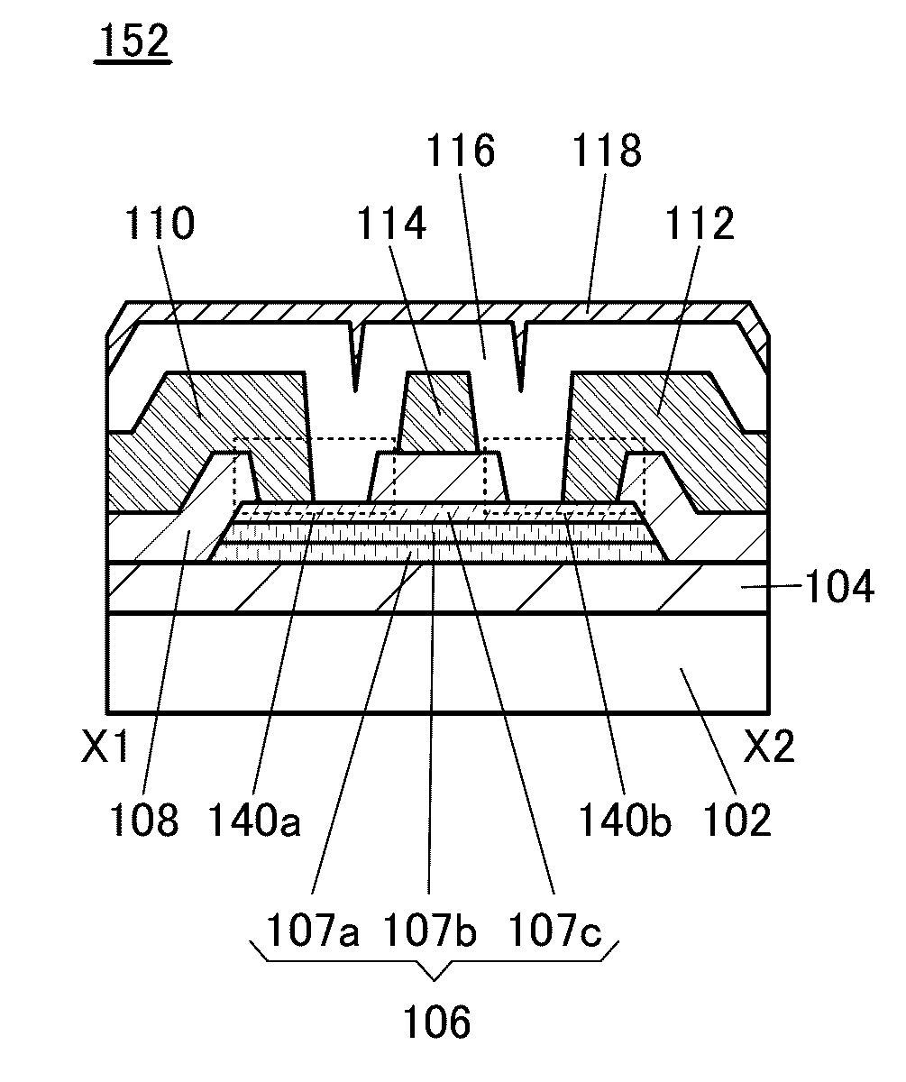
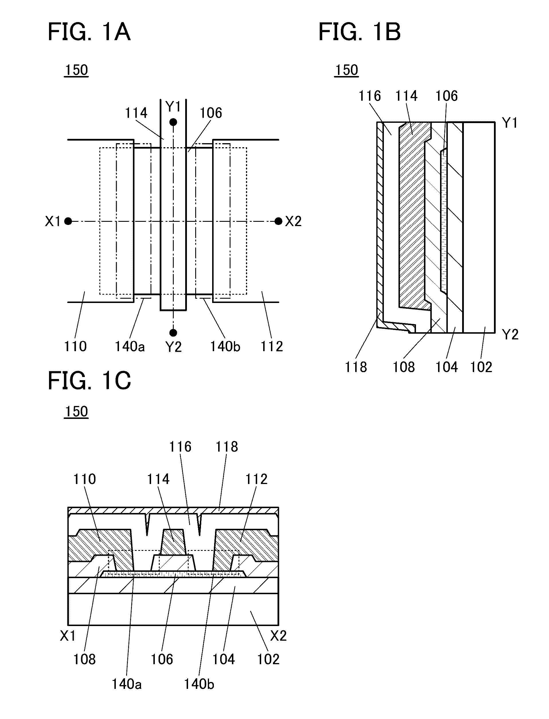
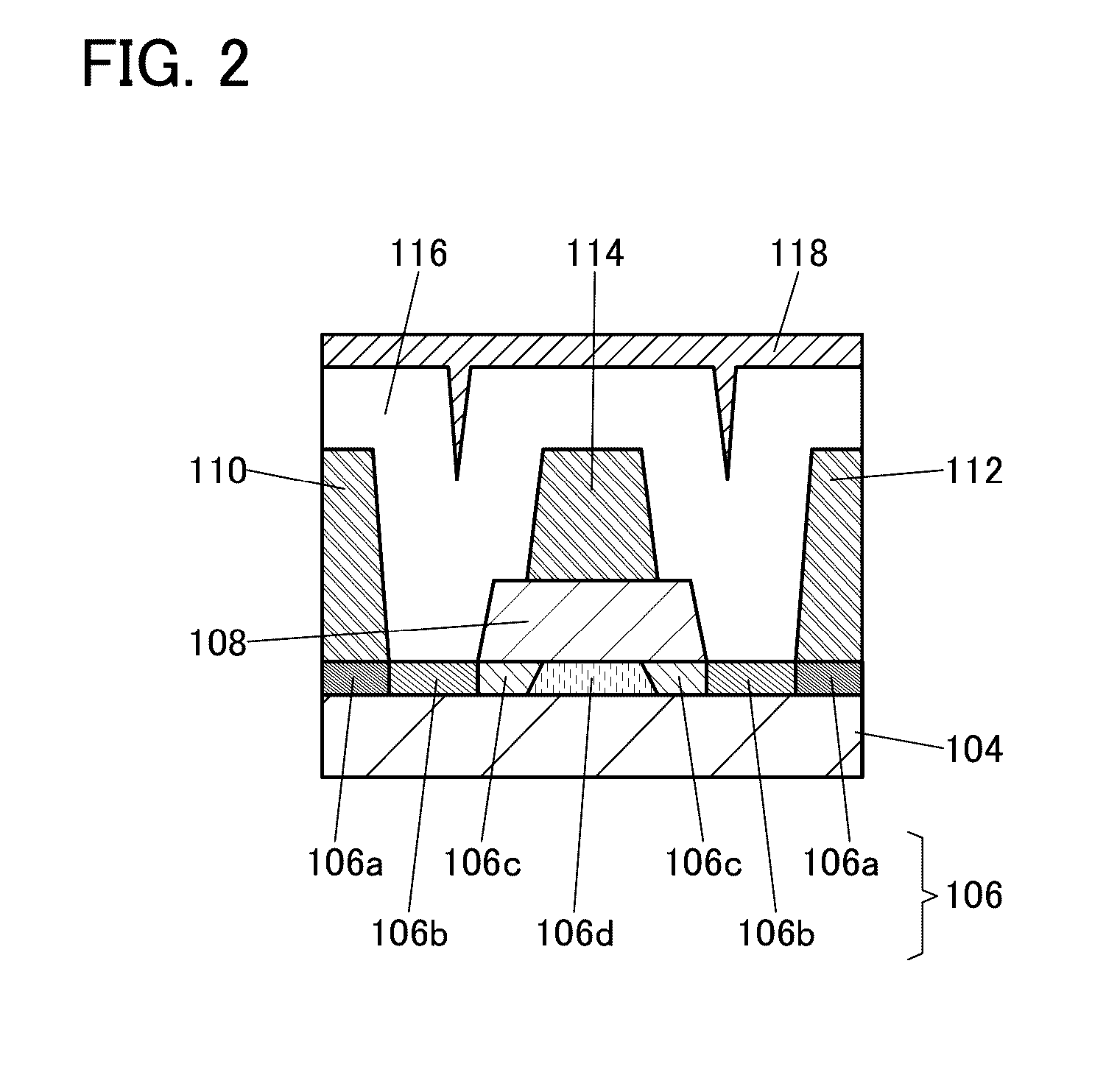
[0077]In FIGS. 1A to 1C, a transistor having a top-gate structure is illustrated as an example of a transistor included in a semiconductor device.

[0078]FIGS. 1A to 1C are a top view and cross-sectional views of a transistor 150 included in a semiconductor device. FIG. 1A is a top view of the transistor 150, FIG. 1B is a cross-sectional view taken along the dashed-dotted line Y1-Y2 in FIG. 1A, and FIG. 1C is a cross-sectional view taken along the dashed dotted line X1-X2 in FIG. 1A. Note that in FIG. 1A, a substrate 102, an insulating film 104, an insulating film 108, an insulating film 116, an insulating film 118,...

embodiment 2

[0282]In this embodiment, one embodiment of a semiconductor device and one embodiment of a method for manufacturing the semiconductor device are described with reference to FIGS. 12A to 12C, FIG. 13, FIGS. 14A to 14C, FIGS. 15A to 15C, FIGS. 16A to 16C, FIGS. 17A to 17C, FIGS. 18A and 18B, FIGS. 19A to 19D, FIGS. 20A and 20B, FIGS. 21A to 21C, and FIGS. 22A to 22C. Note that the difference between this embodiment and Embodiment 1 is in a method for forming the low-resistance region.

5 of Semiconductor Device>

[0283]In FIGS. 12A to 12C, a transistor having a top-gate structure is illustrated as an example of a transistor included in a semiconductor device.

[0284]FIGS. 12A to 12C are a top view and cross-sectional views of a transistor 190 included in a semiconductor device. FIG. 12A is a top view of the transistor 190, FIG. 12B is a cross-sectional view taken along the dashed-dotted line Y1-Y2 in FIG. 12A, and FIG. 12C is a cross-sectional view taken along the dashed-dotted line X1-X2 i...

embodiment 3

[0397]In this embodiment, one embodiment of a semiconductor device and one embodiment of a method for manufacturing the semiconductor device are described with reference to FIGS. 23A and 23B and FIGS. 24A and 24B.

11 of Semiconductor Device>

[0398]FIGS. 23A and 23B illustrate structures of the transistor 150 and a capacitor 159 connected to the transistor 150, which are included in a semiconductor device.

[0399]FIGS. 23A and 23B are a top view and a cross-sectional view of the transistor 150 and the capacitor 159 included in the semiconductor device. FIG. 23A is a top view of the transistor 150 and the capacitor 159. FIG. 23B shows cross sections taken along the dashed-dotted lines X1-X2 and X3-X4 in FIG. 23A. Note that in FIG. 23A, the substrate 102, the insulating films 104, 108, 116, 118, and 122, and the like are omitted for simplicity.

[0400]The transistor 150 illustrated in FIGS. 23A and 23B has a structure similar to that of the transistor 150 in Embodiment 1.

[0401]The capacitor ...


PUM


Abstract

A novel semiconductor device including an oxide semiconductor is provided. In particular, a planar semiconductor device including an oxide semiconductor is provided. A semiconductor device including an oxide semiconductor and having large on-state current is provided. The semiconductor device includes an oxide insulating film, an oxide semiconductor film over the oxide insulating film, a source electrode and a drain electrode in contact with the oxide semiconductor film, a gate insulating film between the source electrode and the drain electrode, and a gate electrode overlapping the oxide semiconductor film with the gate insulating film. The oxide semiconductor film includes a first region overlapped with the gate electrode and a second region not overlapped with the gate electrode, the source electrode, and the drain electrode. The first region and the second region have different impurity element concentrations. The gate electrode, the source electrode, and the drain electrode contain the same metal element.

Description

BACKGROUND OF THE INVENTION[0001]1. Field of the Invention[0002]One embodiment of the present invention relates to a semiconductor device including an oxide semiconductor film and a display device including the semiconductor device.[0003]Note that one embodiment of the present invention is not limited to the above technical field. The technical field of one embodiment of the invention disclosed in this specification and the like relates to an object, a method, or a manufacturing method. In addition, the present invention relates to a process, a machine, manufacture, or a composition of matter. In particular, the present invention relates to a semiconductor device, a display device, a light-emitting device, a power storage device, a storage device, a driving method thereof, or a manufacturing method thereof.[0004]Note that in this specification and the like, a semiconductor device refers to any device that can function by utilizing semiconductor characteristics. A semiconductor eleme...

Claims


Application Information

Patent Timeline
Patent Type & Authority Patents(United States)
IPC IPC(8): H01L29/10H01L29/786H01L29/45H01L29/66H01L29/12H01L27/12H01L29/417H01L29/49H05B44/00
CPCH01L29/7869H01L27/1225H01L29/41733H01L29/45H01L29/4908H01L29/66969H01L29/78621H01L29/78627H01L29/78696H01L2029/7863H10K59/1213H01L29/24
Inventor KOEZUKA, JUNICHIJINTYOU, MASAMISHIMA, YUKINORIHAMOCHI, TAKASHINAKAZAWA, YASUTAKAYAMAZAKI, SHUNPEI
Owner SEMICON ENERGY LAB CO LTD
Why Eureka
Try Eureka