Semiconductor device, manufacturing method thereof, module, and electronic device

a technology of semiconductor devices and manufacturing methods, applied in semiconductor devices, electrical devices, capacitors, etc., can solve the problems of inability to store written data to pixel, inability to manufacture inverted staggered transistors, image quality degradation of display devices, etc., to achieve low manufacturing cost of inverted staggered transistors, the effect of reducing the cost of manufacturing

Active Publication Date: 2017-05-16
SEMICON ENERGY LAB CO LTD
View PDF161 Cites 7 Cited by
  • Summary
  • Abstract
  • Description
  • Claims
  • Application Information

AI Technical Summary

Benefits of technology

[0008]As a transistor including an oxide semiconductor film, an inverted staggered transistor (also referred to as a transistor having a bottom-gate structure), a planar transistor (also referred to as a transistor having a top-gate structure), and the like are given. In the case where a transistor including an oxide semiconductor film is used for a display device, an inverted staggered transistor is used more often than a planar transistor because a manufacturing process of the inverted staggered transistor is relatively simple and manufacturing cost of the inverted staggered transistor can be kept low. However, signal delay or the like is increased by parasitic capacitance that exists between a gate electrode and source and drain electrodes of an inverted staggered transistor and accordingly image quality of a display device degrades, which has posed a problem, as an increase in screen size of a display device proceeds, or a display device is provided with a higher resolution image (for example, a high-resolution display device typified by 4 k×2 k pixels (3840 pixels in the horizontal direction and 2048 pixels in the perpendicular direction) or 8 k×4 k pixels (7680 pixels in the horizontal direction and 4320 pixels in the perpendicular direction)). Furthermore, as another problem, the occupation area of an inverted staggered transistor is larger than that of a planar transistor. Thus, with regard to a planar transistor including an oxide semiconductor film, development of a transistor which has a structure with stable semiconductor characteristics and high reliability and which is formed by a simple manufacturing process is desired.
[0010]In view of the foregoing problems, an object of one embodiment of the present invention is to provide a novel semiconductor device including an oxide semiconductor, particularly to provide a planar type semiconductor device including an oxide semiconductor. Another object is to provide a semiconductor device including an oxide semiconductor and having large on-state current, to provide a semiconductor device including an oxide semiconductor and having small off-state current, to provide a semiconductor device including an oxide semiconductor and occupying a small area, to provide a semiconductor device including an oxide semiconductor and having a stable electrical characteristic, to provide a semiconductor device including an oxide semiconductor and having high reliability, or to provide a novel semiconductor device.
[0021]One embodiment of the present invention can provide a novel semiconductor device including an oxide semiconductor. In particular, a planar type semiconductor device including an oxide semiconductor can be provided. A semiconductor device including an oxide semiconductor and having large on-state current can be provided. A semiconductor device including an oxide semiconductor and having small off-state current can be provided. A semiconductor device including an oxide semiconductor and occupying a small area can be provided. A semiconductor device including an oxide semiconductor and having a stable electrical characteristic can be provided. A semiconductor device including an oxide semiconductor and having high reliability can be provided. A novel semiconductor device can be provided.

Problems solved by technology

However, signal delay or the like is increased by parasitic capacitance that exists between a gate electrode and source and drain electrodes of an inverted staggered transistor and accordingly image quality of a display device degrades, which has posed a problem, as an increase in screen size of a display device proceeds, or a display device is provided with a higher resolution image (for example, a high-resolution display device typified by 4 k×2 k pixels (3840 pixels in the horizontal direction and 2048 pixels in the perpendicular direction) or 8 k×4 k pixels (7680 pixels in the horizontal direction and 4320 pixels in the perpendicular direction)).
Furthermore, as another problem, the occupation area of an inverted staggered transistor is larger than that of a planar transistor.
Depending on the structure of the capacitor, there has been a problem in that data written to the pixel cannot be stored and the image quality of the display device is degraded.

Method used


Image

  • Semiconductor device, manufacturing method thereof, module, and electronic device
  • Semiconductor device, manufacturing method thereof, module, and electronic device
  • Semiconductor device, manufacturing method thereof, module, and electronic device

Examples


embodiment 1

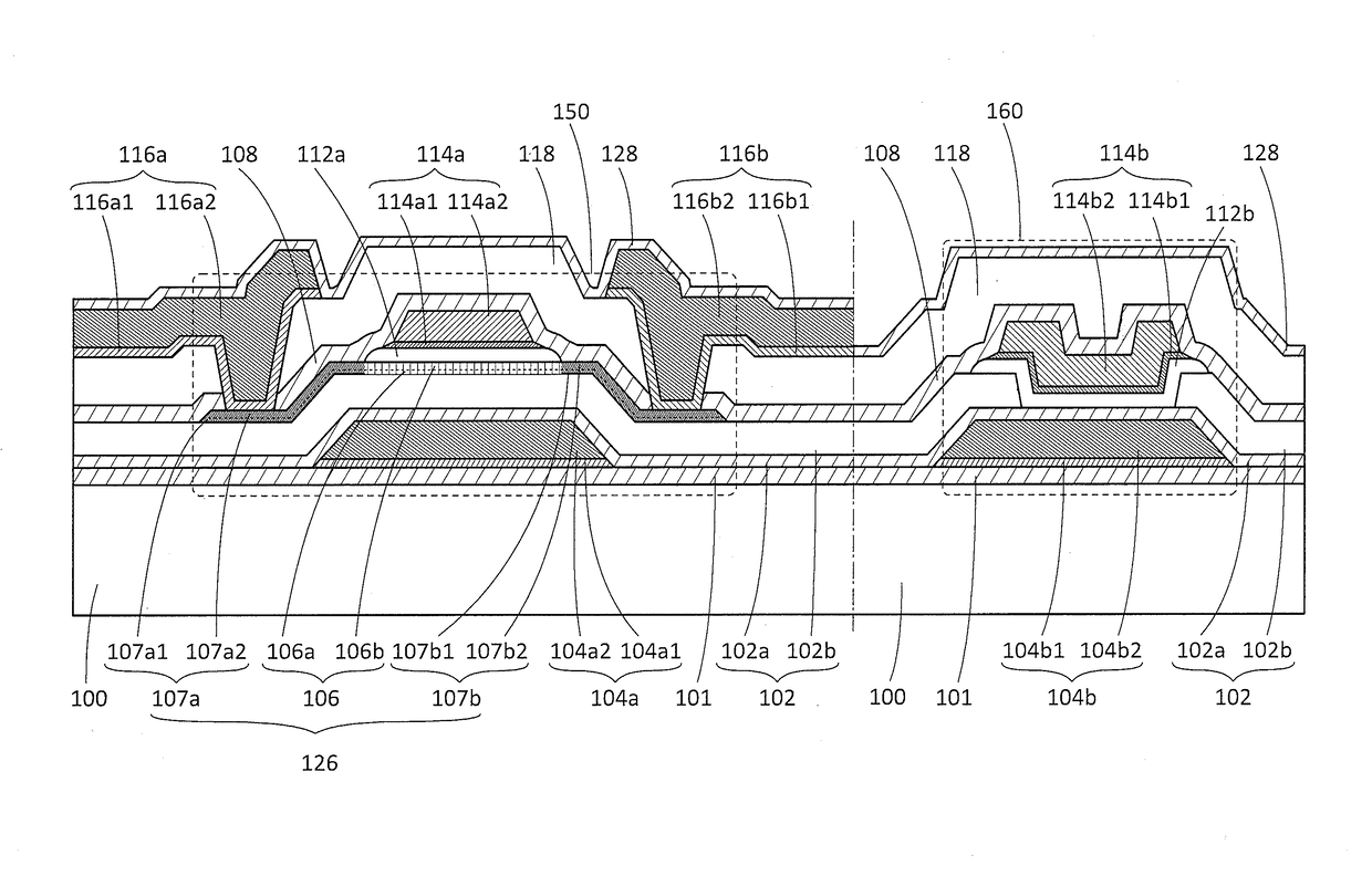
[0095]In this embodiment, one embodiment of a semiconductor device and one embodiment of a method for manufacturing the semiconductor device will be described with reference to drawings.

[0096]FIG. 1 illustrates a transistor having a top-gate structure as an example of a transistor included in a semiconductor device and a capacitor that can be formed in the same process as the transistor.

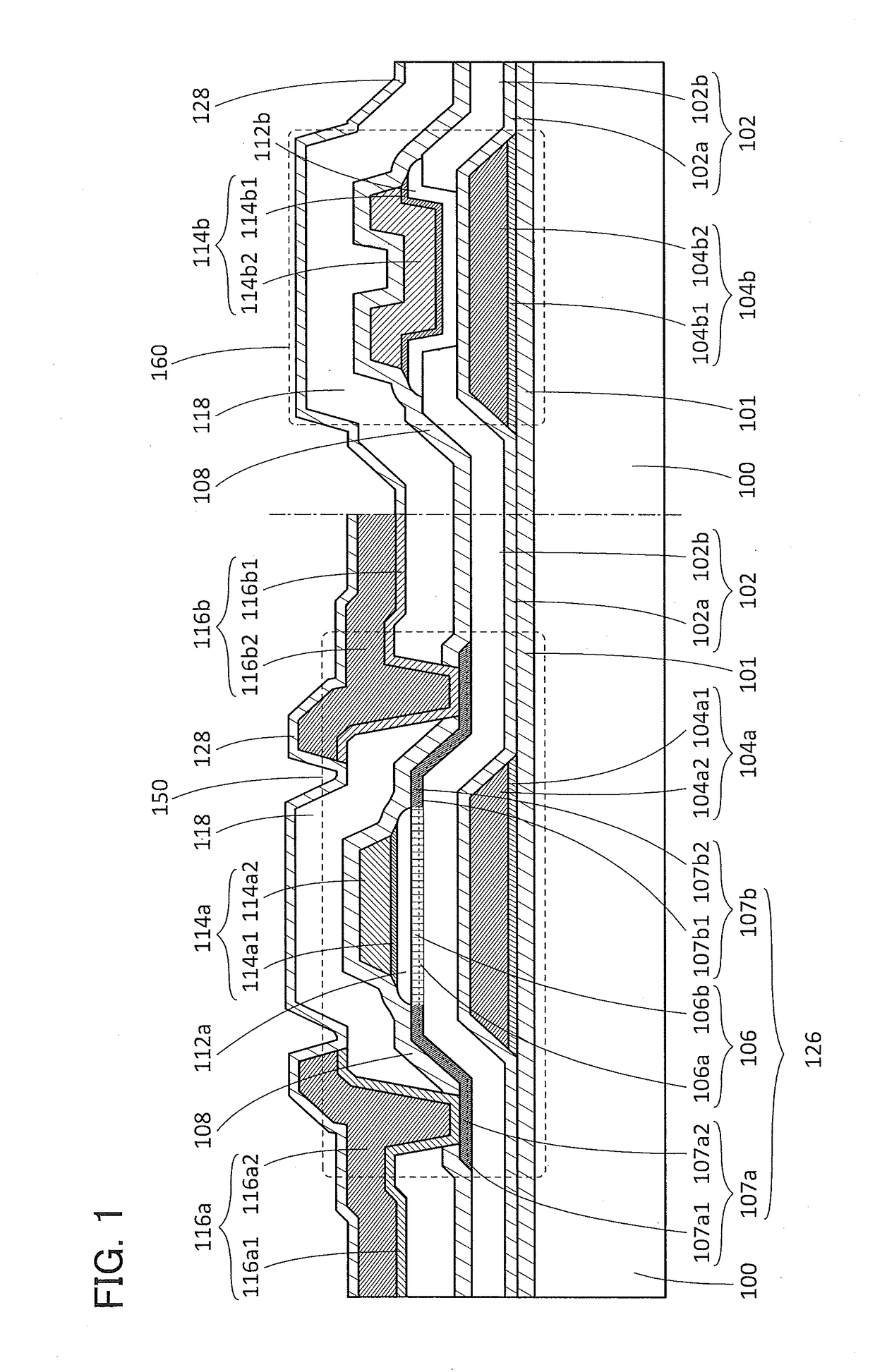
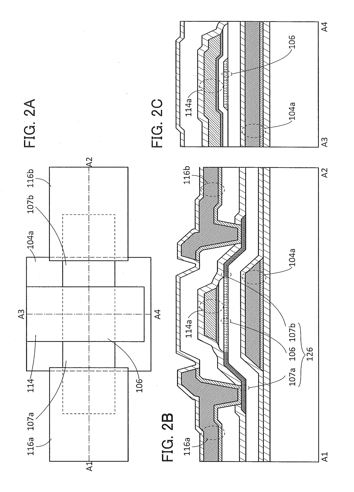
[0097]FIG. 1 is a cross-sectional view of a transistor 150 and a capacitor 160 included in a semiconductor device. FIGS. 2A to 2C are a top view and cross-sectional views of the transistor 150. FIG. 2A is a top view of the transistor 150, FIG. 2B is a cross-sectional view taken along the dashed-dotted line A1-A2 in FIG. 2A, and FIG. 2C is a cross-sectional view taken along the dashed-dotted line A3-A4 in FIG. 2A. Note that in FIG. 2A, a substrate 100, an insulating film 101, an insulating film 102, a gate insulating film 112a, an insulating film 108, an insulating film 118, an insulating film 128, an...

embodiment 2

[0317]In this embodiment, a structure of an oxide semiconductor included in a semiconductor device of one embodiment of the present invention will be described.

[0318]An oxide semiconductor is classified into a single crystal oxide semiconductor and a non-single-crystal oxide semiconductor. Examples of a non-single-crystal oxide semiconductor include a c-axis aligned crystalline oxide semiconductor (CAAC-OS), a polycrystalline oxide semiconductor, a nanocrystalline oxide semiconductor (nc-OS), an amorphous-like oxide semiconductor (a-like OS), and an amorphous oxide semiconductor.

[0319]From another perspective, an oxide semiconductor is classified into an amorphous oxide semiconductor and a crystalline oxide semiconductor. Examples of a crystalline oxide semiconductor include a single crystal oxide semiconductor, a CAAC-OS, a polycrystalline oxide semiconductor, and an nc-OS.

[0320]It is known that an amorphous structure is generally defined as being metastable and unfixed, and being ...

embodiment 3

[0356]In this embodiment, deposition models of a CAAC-OS and an nc-OS will be described.

[0357]FIG. 46A is a schematic view of the inside of a deposition chamber where a CAAC-OS is deposited by sputtering.

[0358]A target 630 is attached to a backing plate. Under the target 630 and the backing plate, a plurality of magnets is placed. The plurality of magnets generates a magnetic field over the target 630. Sputtering in which disposition speed is increased by utilizing a magnetic field of magnets is referred to as magnetron sputtering.

[0359]The target 630 has a polycrystalline structure in which a cleavage plane exists in at least one crystal grain. Note that the details of the cleavage plane will be described later.

[0360]A substrate 620 is placed to face the target 630, and the distance d (also referred to as a target-substrate distance (T-S distance)) is greater than or equal to 0.01 m and less than or equal to 1 m, preferably greater than or equal to 0.02 m and less than or equal to ...


PUM


Abstract

A semiconductor device includes a transistor and a capacitor. The transistor includes a first conductive film; a first insulating film including a film containing hydrogen; a second insulating film including an oxide insulating film; an oxide semiconductor film including a first region and a pair of second regions; a pair of electrodes; a gate insulating film; and a second conductive film. The capacitor includes a lower electrode, an inter-electrode insulating film, and an upper electrode. The lower electrode contains the same material as the first conductive film. The inter-electrode insulating film includes a third insulating film containing the same material as the first insulating film and a fourth insulating film containing the same material as the gate insulating film. The upper electrode contains the same material as the second conductive film. A fifth insulating film containing hydrogen is provided over the transistor.

Description

BACKGROUND OF THE INVENTION[0001]1. Field of the Invention[0002]One embodiment of the present invention relates to a semiconductor device including an oxide semiconductor film, a method for manufacturing the semiconductor device, a module, and an electronic device.[0003]Note that one embodiment of the present invention is not limited to the above technical field. The technical field of one embodiment of the invention disclosed in this specification and the like relates to an object, a method, or a manufacturing method. In addition, the present invention relates to a process, a machine, manufacture, or a composition of matter. In particular, one embodiment of the present invention relates to a semiconductor device, a display device, a light-emitting device, a power storage device, a memory device, a driving method thereof, or a manufacturing method thereof.[0004]In this specification and the like, a semiconductor device generally means a device that can function by utilizing semicond...

Claims


Application Information

Patent Timeline
Patent Type & Authority Patents(United States)
IPC IPC(8): H01L27/12
CPCH01L27/1225H01L27/1255H01L28/60H01L27/1248H01L27/1259H01L29/24H01L29/42384H01L29/4908H01L29/518H01L29/66969H01L29/78618H01L29/7869
Inventor YAMAZAKI, SHUNPEIOKAZAKI, KENICHINAKADA, MASATAKAKATAYAMA, MASAHIRO
Owner SEMICON ENERGY LAB CO LTD
Why Eureka
Try Eureka