

Method for manufacturing semiconductor device
- Summary
- Abstract
- Description
- Claims
- Application Information
AI Technical Summary
Benefits of technology
Problems solved by technology
Method used
Image

Examples
embodiment 1
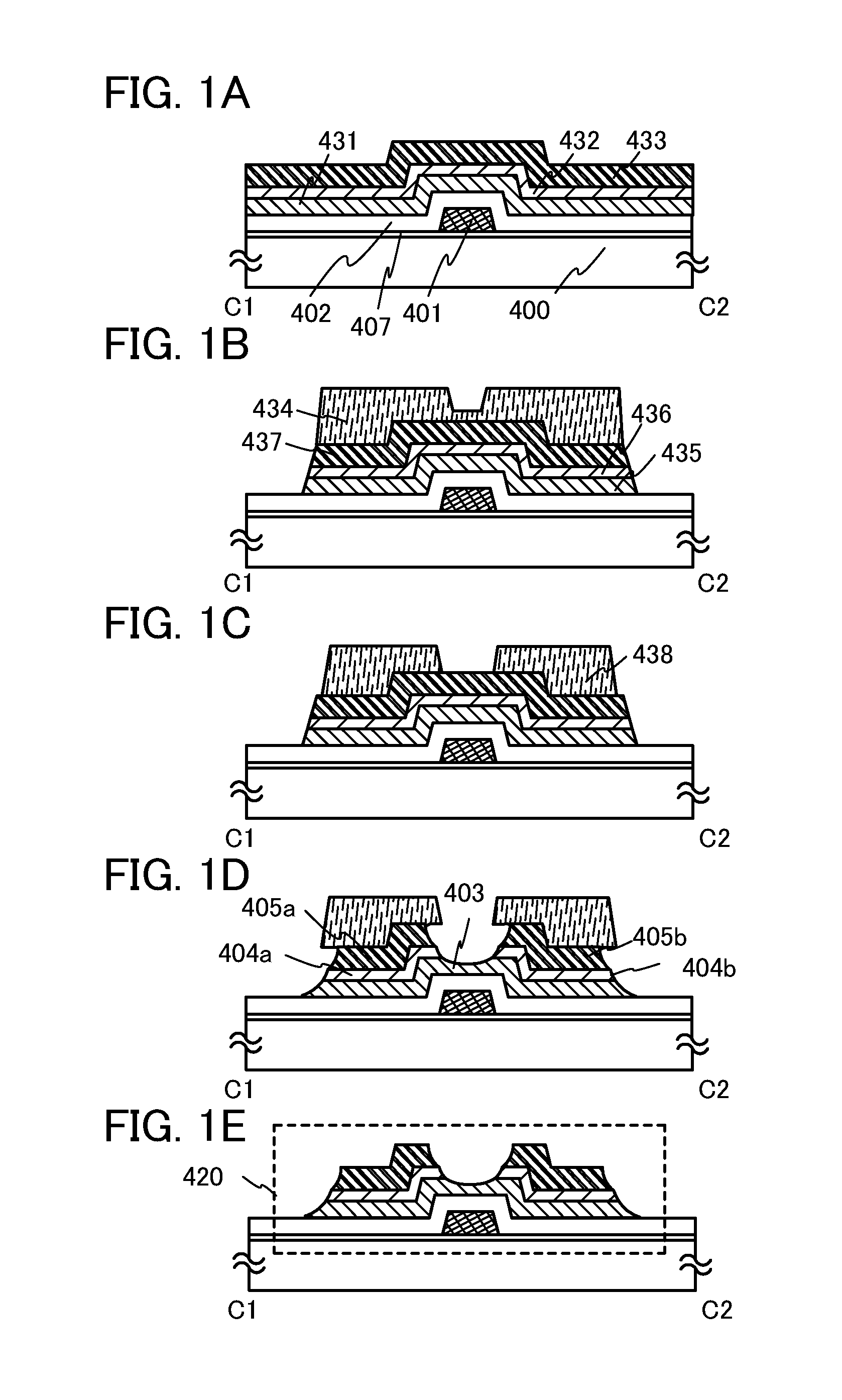
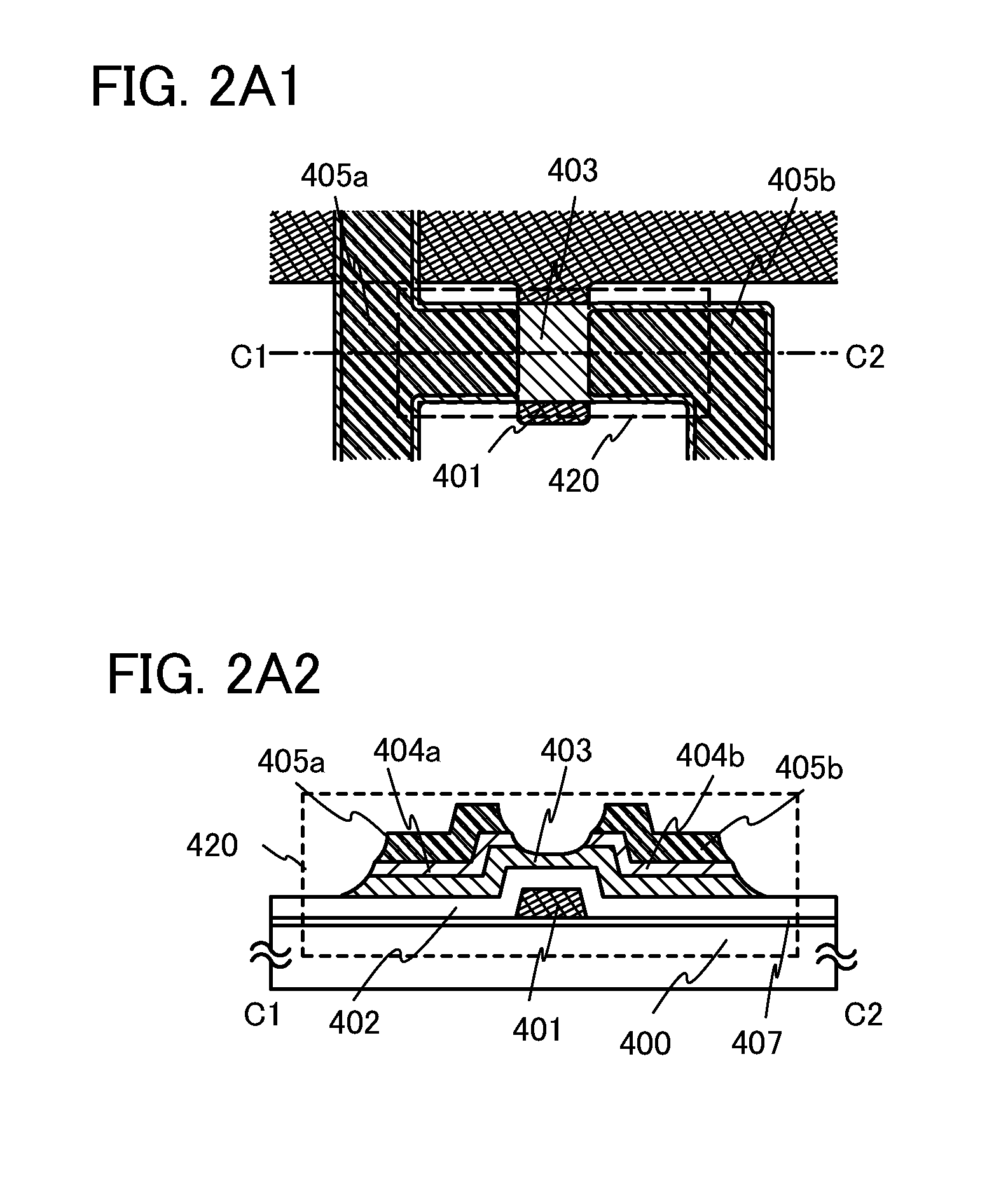
[0064]A method for manufacturing a semiconductor device of this embodiment is described with reference to FIGS. 1A to 1E and FIGS. 2A1 and 2A2.
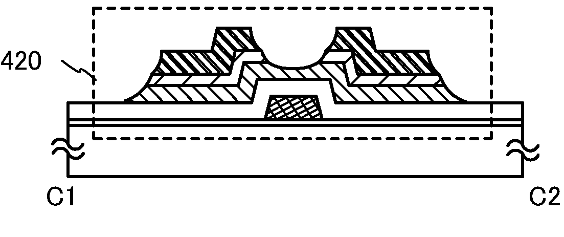
[0065]FIG. 2A1 is a plan view of a thin film transistor 420 of a semiconductor device of this embodiment, and FIG. 2A2 is a cross-sectional view taken along C1-C2 of FIG. 2A1. The thin film transistor 420 is an inverted staggered thin film transistor and includes a gate electrode layer 401, a gate insulating layer 402, a semiconductor layer 403, n layers 404a and 404b serving as a source region and a drain region, and source and drain electrode layers 405a and 405b.
[0066]FIGS. 1A to 1E correspond to cross-sectional views showing steps of manufacturing the thin film transistor 420.
[0067]In FIG. 1A, an insulating film 407 serving as a base film is provided over a substrate 400 and the gate electrode layer 401 is provided over the insulating film 407. The insulating film 407 has a function of preventing diffusion of an impurity element from the...
embodiment 2
[0119]Here, an example of a semiconductor device including a thin film transistor with a structure where the source and drain electrode layers are in contact with the semiconductor layer in Embodiment 1 is described with reference to FIGS. 3A to 3E and FIGS. 4A1 and 4A2.
[0120]FIG. 4A1 is a plan view of a thin film transistor 460 in a semiconductor device of this embodiment, and FIG. 4A2 is a cross-sectional view taken along D1-D2 of FIG. 4A1. The thin film transistor 460 is an inverted staggered thin film transistor and includes a gate electrode layer 451, a gate insulating layer 452, a semiconductor layer 453, and source and drain electrode layers 455a and 455b.
[0121]FIGS. 3A to 3E are cross-sectional views showing steps of manufacturing the thin film transistor 460.
[0122]In FIG. 3A, an insulating film 457 serving as a base film is provided over a substrate 450 and the gate electrode layer 451 is provided over the insulating film 457. In this embodiment, a silicon oxide film (with...
embodiment 3
[0154]In this embodiment, a process for manufacturing a display device including a thin film transistor is described with reference to FIGS. 5A to 5C, FIGS. 6A to 6C, FIG. 7, FIG. 8, FIG. 9, FIG. 10, FIGS. 11A1, 11A2, 11B1, and 11B2, and FIG. 12.
[0155]As for a substrate 100 having a light-transmitting property shown in FIG. 5A, a glass substrate of barium borosilicate glass, aluminoborosilicate glass, or the like which is typified by #7059 glass, #1737 glass, or the like manufactured by Corning, Inc. can be used.
[0156]Next, a conductive layer is formed entirely over a surface of the substrate 100, and then a first photolithography process is performed to form a resist mask. Then, an unnecessary portion is removed by etching, so that wirings and electrodes (a gate wiring including a gate electrode layer 101, a capacitor wiring 108, and a first terminal 121) are formed. At this time, the etching is performed so that at least an end portion of the gate electrode layer 101 is tapered. F...
PUM
 Abstract
Description
Claims
Application Information