Red light semiconductor area array light source device for laser display

A light source device and laser display technology, which is applied in the direction of semiconductor lasers, lasers, projection devices, etc., can solve the problems of large volume of projection display optical system, unsatisfactory decoherence effect, and difficult output beam shaping, so as to reduce optical elements and improve The effect of light energy utilization and low power consumption

Inactive Publication Date: 2013-11-27
INST OF SEMICONDUCTORS - CHINESE ACAD OF SCI
View PDF4 Cites 25 Cited by
  • Summary
  • Abstract
  • Description
  • Claims
  • Application Information

AI Technical Summary

Problems solved by technology

[0009] The present invention aims to solve the problems of the existing laser projection display system. Due to the large volume of the laser light source, the difficulty in shaping the output beam, the complexity of the uniform light system, and the unsatisfactory decoherence effect, the projection display optical system is large in size, low in light energy utilization, and power Large, and the strong laser interference leads to the formation of speckles and other problems

Method used


Image

  • Red light semiconductor area array light source device for laser display
  • Red light semiconductor area array light source device for laser display
  • Red light semiconductor area array light source device for laser display

Examples


Embodiment Construction

[0021] In order to make the object, technical solution and advantages of the present invention clearer, the present invention will be further described in detail below in conjunction with specific embodiments and with reference to the accompanying drawings.

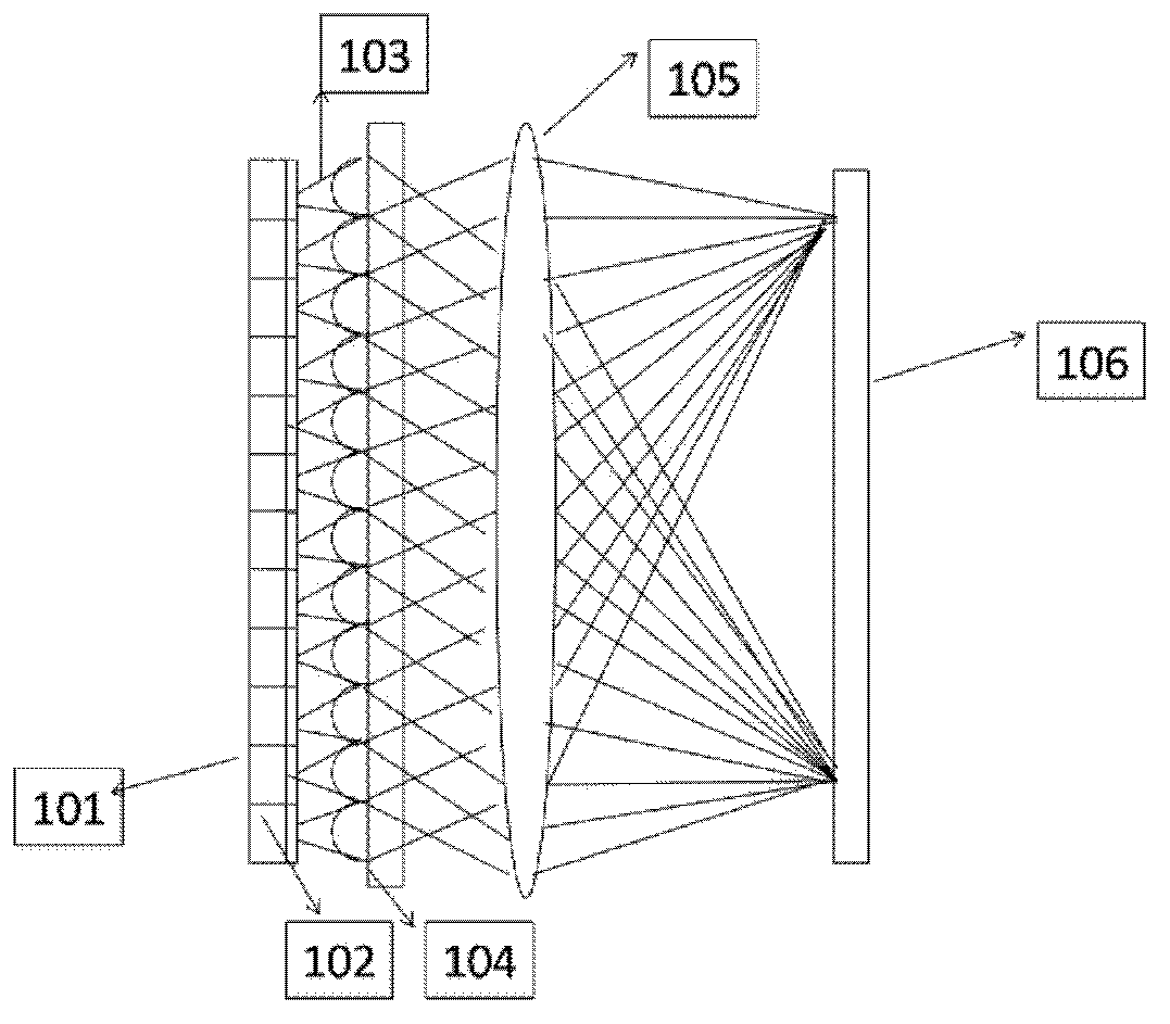
[0022] see figure 1 As shown, the present invention provides a red light semiconductor area array light source device for laser display, which includes:

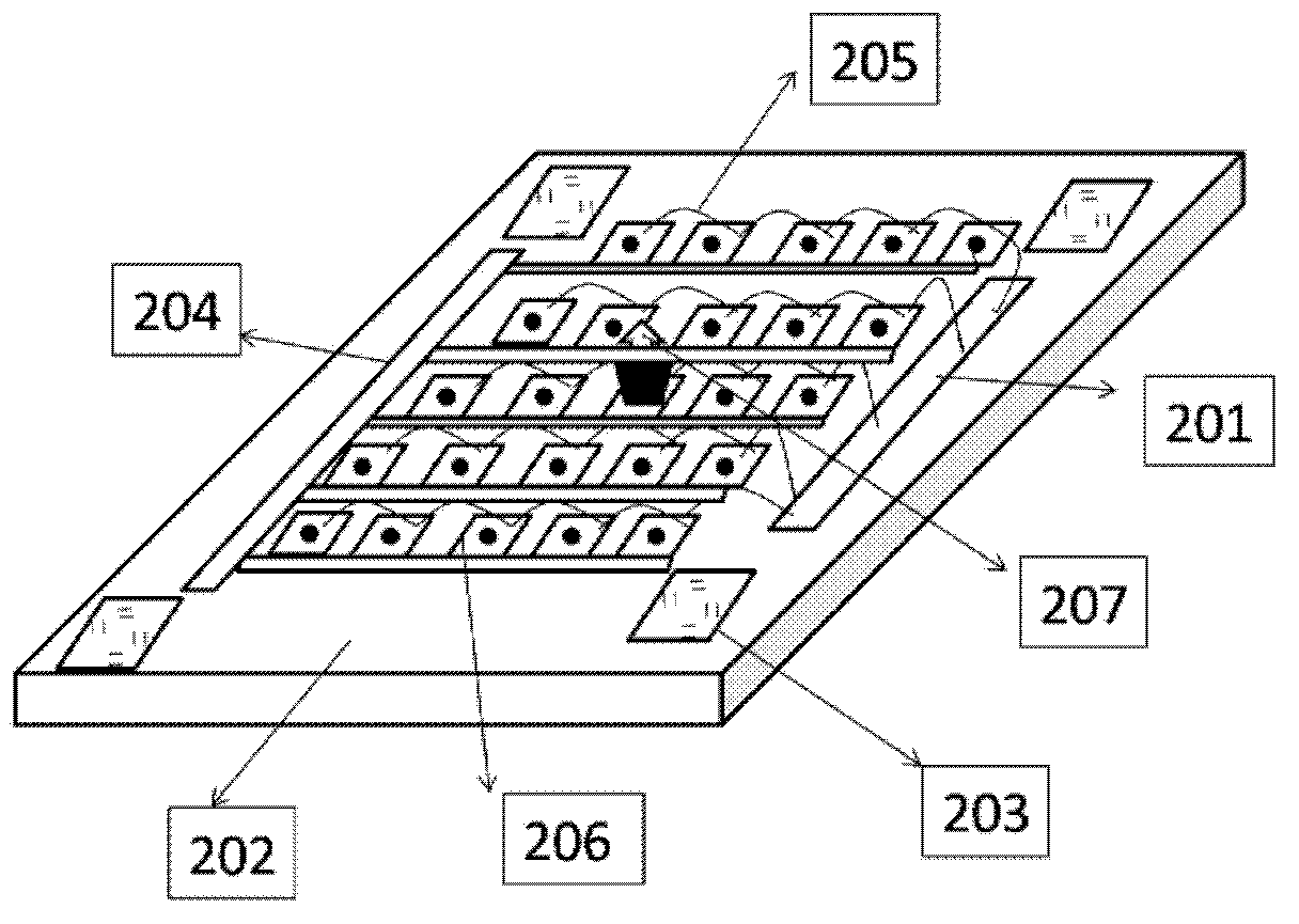
[0023] A VCSEL array 101, which is used to output circular laser beams, and the spatial coherence of the beams output by multiple VCSELs is weakened, thereby weakening the influence of laser speckle on the laser projection display system, thereby playing a role of decoherence ;The array packaging method refers to figure 2 As shown, it is an N×M surface array composed of a plurality of VCSEL chip units 102, and the number of chips in the length and width directions is determined to be 16:9; The optical path is simplified, and the utilization rate of light energy is im...


PUM


Abstract

The invention discloses a red light semiconductor area array light source device for laser display. The red light semiconductor area array light source device for laser display comprises a VCSEL area array and a microlens array, wherein the VCSEL area array at least comprises a plurality of VCSEL units which are used for emitting circular laser beams, and the microlens array is formed by a plurality of microlens and used for performing collimation rounding on the laser beams output by the VCSEL area array and outputting the laser beams. The light source device can reduce optical elements in a projection display optical path, shorten the length of a lighting optical path, and improve the optical energy utilization rate. In addition, the VCSEL area array can reduce interference between VCSEL lasers and weaken laser speckles, and therefore projection display quality is improved. According to the red light semiconductor area array light source device, the area array light source packaging technology and VCSEL are adopted, a two-dimensional array is easy to integrate, and the defect that power transmitted by a single tube is poor can be overcome. The VCSEL is available in wafer test, reduces cost greatly and is easy in modularization and packaging.

Description

technical field [0001] The invention belongs to the field of semiconductor laser light sources for laser display, in particular to a red light semiconductor surface array light source device for laser display and a manufacturing method thereof. Background technique [0002] At present, the laser display using semiconductor laser as the light source is regarded as the fourth generation display of the color revolution due to its large color gamut, rich colors, high color saturation, and strong expressiveness; the life of the light source is as long as tens of thousands of hours; and the power consumption is low. Technology, known as "the revolution in the history of human vision". Compared with solid-state lasers, it is compact in size and less affected by temperature. With the commercialization of the direct lasing green semiconductor laser LD, portable (compact), high-efficiency laser display systems will seize markets such as home theaters, miniature projection displays, a...

Claims


Application Information

Patent Timeline
Patent Type & Authority Applications(China)
IPC IPC(8): G02B27/09G02B27/48G03B21/20H01S5/183H01S5/42
Inventor 孔庆善董辉张运方方青刘育梁
Owner INST OF SEMICONDUCTORS - CHINESE ACAD OF SCI
Why Eureka
Try Eureka