

Semiconductor device, method of manufacturing same, and method of controlling semiconductor device
A semiconductor and device technology, which is used in the field of controlling semiconductor devices to achieve the effect of improving image quality
- Summary
- Abstract
- Description
- Claims
- Application Information
AI Technical Summary
Problems solved by technology
Method used
Image

Examples
no. 1 example
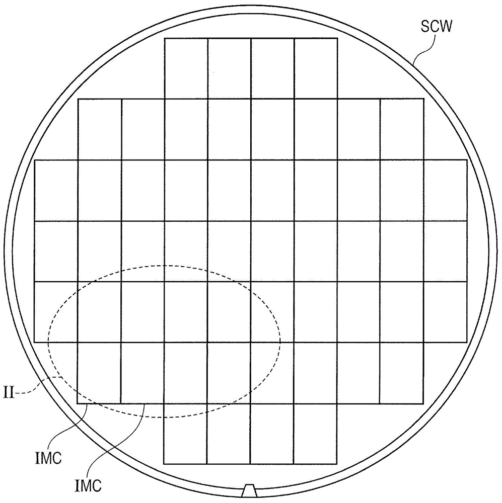
[0062] First, refer to figure 1 and figure 2 A semiconductor device in the form of a wafer of the present embodiment is described.
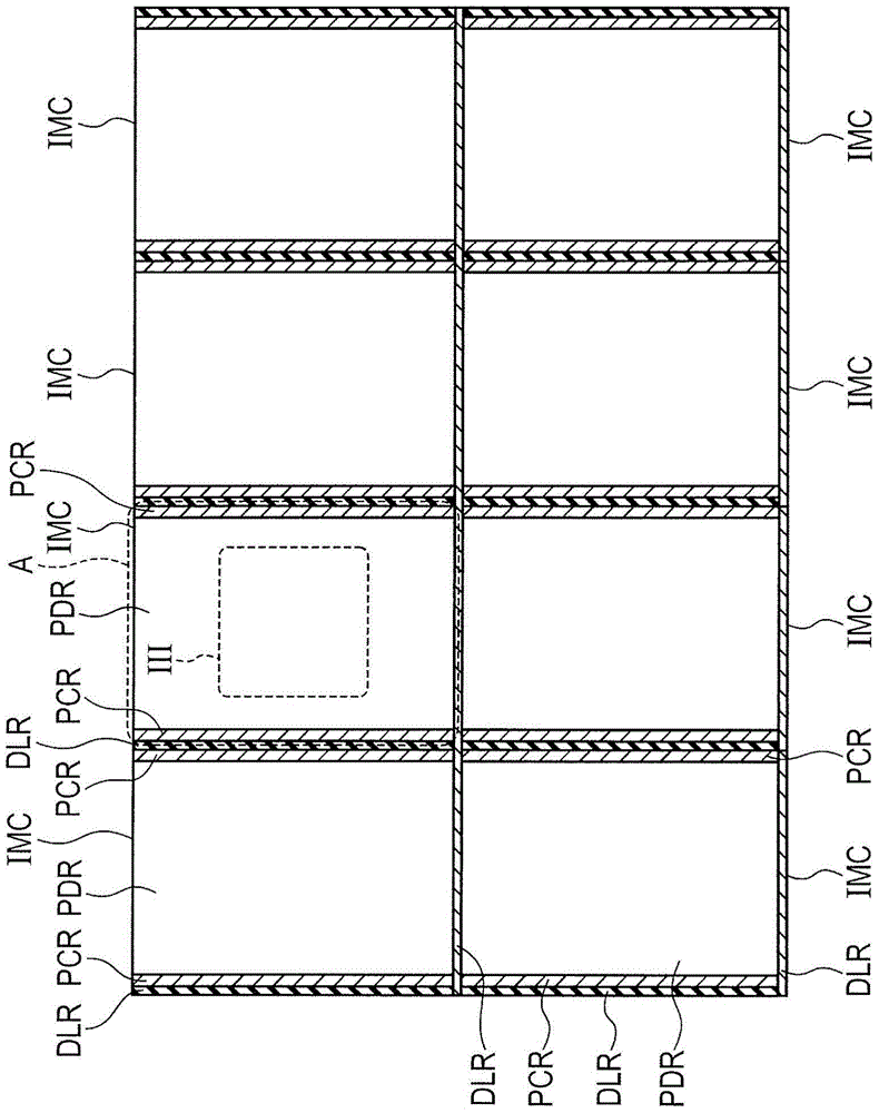
[0063] like figure 1 As shown, the semiconductor wafer SCW has a plurality of chip regions IMC for image sensors. The chip regions IMC each have a rectangular planar shape, and they are placed in a matrix.
[0064] like figure 2 As shown, the chip area IMC has, as a photoelectric conversion element, for example, a pixel portion PDR and a peripheral circuit portion PCR, wherein the pixel portion PDR is a formation area of a photodiode, and the peripheral circuit portion PCR is a formation area of a peripheral circuit for controlling the photodiode. . The peripheral circuit portion PCR is located, for example, on both sides of the pixel portion PDR. The chip area IMC has a scribe line area DLR therebetween. The scribe line region DLR has alignment marks therein. By dicing along this scribe line region DLR, the semiconductor wafer SC...
no. 2 example
[0162] like Figure 28 As shown, the present embodiment uses the element isolation insulating film SI made of, for example, a silicon oxide film and formed of LOCOS (Local Oxidation of Silicon), instead of the element isolation insulating film SI of the first embodiment formed of STI.
[0163] The second embodiment differs from the first embodiment in the above-mentioned points, but the configuration of this embodiment is almost similar to that of the first embodiment other than that. exist Figure 28 In , similar elements are identified by similar reference numerals and overlapping descriptions are omitted. Also in this embodiment, substantially similar advantageous effects as those of the first embodiment can be obtained.
[0164] like Figure 29 As shown, in the manufacturing method of this embodiment, for example, the silicon nitride oxide film NOF is formed by CVD or the like instead of Figure 5 The silicon oxide film OX is formed on substantially the entire main sur...
no. 3 example
[0169] like Figure 32 As shown, the present embodiment has an element isolation insulating film DI called a DTI (Deep Trench Isolation) film instead of the element isolation insulating film SI formed by STI in the first embodiment, and the element isolation insulating film DI is formed on the main surface S2 The side extends deeper than the element isolation insulating film SI, and is made of, for example, a silicon oxide film.
[0170] Similar to the element isolation insulating film SI, the element isolation insulating film DI is preferably formed at a boundary portion between one pixel region and another pixel region adjacent thereto. For example, it may be formed in main surface S1 in at least part of a region overlapping with p-type well region DPW3 located in the pixel boundary region in plan view. The element isolation insulating film DI preferably extends to the main surface S2 side deeper than the lowermost part of the p-type well region DPW1 of the pixel region (...
PUM
 Abstract
Description
Claims
Application Information