Logic delay locking based anti-interference circuit and method

A logic delay and delay circuit technology, applied in the direction of single output arrangement, etc., can solve the problems of time jitter, affecting the quality of trigger signals, and electronic equipment cannot be accurately triggered, so as to achieve the effect of suppressing signal interference signals

Inactive Publication Date: 2015-09-16
INST OF FLUID PHYSICS CHINA ACAD OF ENG PHYSICS
View PDF4 Cites 3 Cited by
  • Summary
  • Abstract
  • Description
  • Claims
  • Application Information

AI Technical Summary

Problems solved by technology

[0003] Commonly used suppression measures such as shielding and filtering will always bring additional hardware costs, and may affect the quality of the trigger signal, especially the timing jitter, so that the electronic device cannot be accurately triggered

Method used


Image

  • Logic delay locking based anti-interference circuit and method
  • Logic delay locking based anti-interference circuit and method

Examples


Embodiment 1

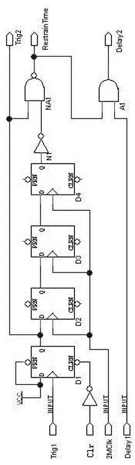
[0039] Embodiment 1: as figure 1 shown. The circuit includes 4 D flip-flops (where D1 is used as a step signal generator, and the delay circuit includes flip-flop D2, flip-flop D3, and flip-flop D4), 2 inverters, 1 NAND gate and 1 AND gate . The trigger signal Trig1 is connected to the clock input terminal of the trigger D1, the output terminal of the trigger D1 is connected to the signal input terminal of the trigger D2, the output terminal of the trigger D2 is connected to the signal input terminal of the trigger D3, and the output terminal of the trigger D3 is connected to the signal input terminal of the trigger D4 The signal input terminals are connected, and the clock signal 2MClk is connected with the clock input terminals of flip-flops D2-D4 at the same time. The output terminal of the trigger D4 is connected to the input terminal of the inverter N1, the output terminal of the inverter N1 is connected to one input terminal of the NAND gate NA1, the output terminal of...


PUM


Abstract

The invention relates to the field of data acquiring, in particular relates to a logic delay locking based anti-interference circuit and method, and aims at solving the problems in the prior art. The circuit and method are that a leading edge of a triggering signal is treated as a time reference point to lock an interference signal within a fixed delay range, so as to solve the interference problem related to a time sequence of the triggering signal. According to the circuit and method, a D triggering device is used for converting the triggering signal into a step signal which is synchronous with the leading edge; then a plurality of D triggering devices, a phase inverter and an NAND gate are used for converting the step signal into an inversion signal, wherein the leading time of the inversion signal is the same as that of the triggering signal, and the pulse width is determined by a clock cycle and the number of the D triggering devices; if the delay time of the interference relative to the triggering signal is less than the pulse width, the signal and the interference signal AND can be utilized to inhibit the interference signal within the pulse width.

Description

technical field [0001] The invention relates to the field of data acquisition, in particular to an anti-jamming circuit and method based on logic delay locking. Background technique [0002] In some physical experiments, the trigger signal used to trigger electronic equipment is often accompanied by interference signals. For example, when multiple synchronous trigger signals are used to simultaneously trigger high-power pulse devices and electronic equipment, the interference signals generated by the action of high-power pulse devices will affect the normal operation of electronic equipment. The characteristics of these interference signals are: coming immediately after the trigger, and the duration is short (for example, less than 1μS). After the action of the high-power pulse device, some physical quantities need to be measured or processed, and the signals representing these physical quantities generally arrive after a certain delay time (for example, greater than 1.5μS)...

Claims


Application Information

Patent Timeline
Patent Type & Authority Applications(China)
IPC IPC(8): H03K5/13
Inventor 叶超李洪涛谢敏李亚维龙燕
Owner INST OF FLUID PHYSICS CHINA ACAD OF ENG PHYSICS
Why Eureka
Try Eureka