On Cell structure touch display screen and manufacturing method thereof and display device

A technology of a touch display screen and a manufacturing method, which are applied in the fields of display devices, touch display screens and manufacturing methods thereof, can solve the problem of high error reporting rate of an exposure machine, and achieve the effect of improving the alignment accuracy and low

Active Publication Date: 2015-12-23
BOE TECH GRP CO LTD +1
View PDF8 Cites 12 Cited by
  • Summary
  • Abstract
  • Description
  • Claims
  • Application Information

AI Technical Summary

Problems solved by technology

[0005] The object of the present invention is to provide an OnCell structure touch display screen, its manufacturing method, and display devi

Method used


Image

  • On Cell structure touch display screen and manufacturing method thereof and display device
  • On Cell structure touch display screen and manufacturing method thereof and display device
  • On Cell structure touch display screen and manufacturing method thereof and display device

Examples


Embodiment Construction

[0034] In order to further illustrate the OnCell structure touch display screen provided by the embodiments of the present invention, its manufacturing method, and display device, the present invention will be further described in detail below in conjunction with the accompanying drawings.

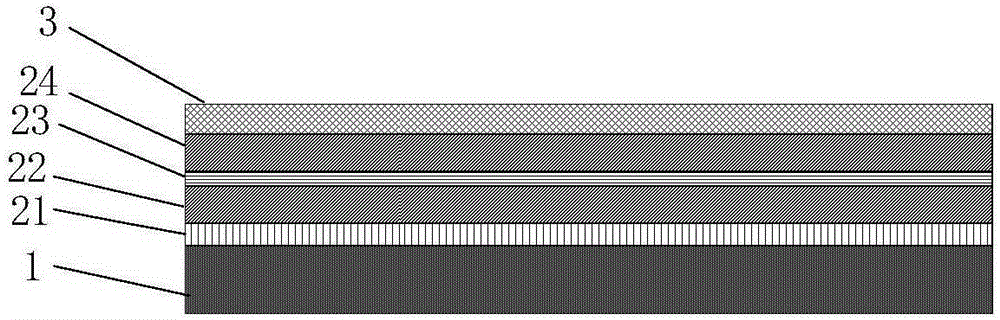
[0035] see figure 1 The method for manufacturing an OnCell structure touch display screen provided by an embodiment of the present invention specifically includes: sequentially manufacturing a transparent semiconductor layer 21 , a first protective layer 22 , and a metal layer 23 along the direction of light propagation between the color filter substrate 1 and the polarizer 3 and the second protective layer 24; wherein,

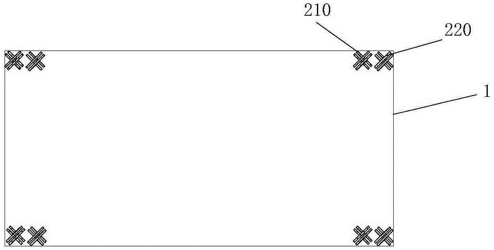
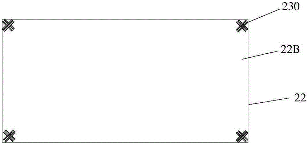
[0036] see Figure 2-4 The alignment marks 210 of the transparent semiconductor layer and the alignment marks 220 of the first protective layer are all made on the black matrix of the color filter substrate 1; the alignment marks 210 of the transparent semiconductor laye...


PUM

PropertyMeasurementUnit
Thicknessaaaaaaaaaa
Thicknessaaaaaaaaaa

Abstract

The invention discloses an On Cell structure touch display screen and a manufacturing method thereof and a display device, relates to the technical field of liquid crystal display, and aims at solving the problem of high error-reporting rate of an exposure machine in the process of alignment exposure on a plurality of touch layers. The manufacturing method of the On Cell structure touch display screen comprises the steps as follows: a transparent semiconductor layer, a first protection layer, a metal layer and a second protection layer are sequentially manufactured between a color-film substrate and a polarizing plate along a ray propagation direction; alignment marks of the transparent semiconductor layer and the first protection layer are manufactured on a black matrix of the color-film substrate; the used materials are light-shielding materials; the alignment mark of the metal layer is made of a photoresist; and the alignment mark of the second protection layer is made of a reflecting material. The On Cell structure touch display screen is manufactured by the manufacturing method; and the manufacturing method of the On Cell structure touch display screen disclosed by the invention is used for manufacturing the touch screen.

Description

technical field [0001] The invention relates to the technical field of liquid crystal display, in particular to a touch display screen with an OnCell structure, a manufacturing method thereof, and a display device. Background technique [0002] At present, with the development of liquid crystal display technology, people put forward higher and higher requirements for the human-computer interaction function of the liquid crystal display. However, in the existing technology, people generally use the OnCell technology to combine a traditional liquid crystal display screen with a touch sensor to form an OnCell structure touch screen, so as to improve the human-computer interaction function of the liquid crystal display. [0003] Specifically, Oncell technology refers to the method of embedding the touch layer between the color filter substrate and the polarizer of the liquid crystal display, and can be divided into a single-layer touch layer and a multi-layer touch layer accordi...

Claims


Application Information

Patent Timeline
IPC IPC(8): G03F7/20G02F1/1335G02F1/1333G02F1/13
Inventor 丁贤林许邹明胡明谢涛峰李可丰
Owner BOE TECH GRP CO LTD
Why Eureka
Try Eureka