Conductive thin film

A conductive thin film and thin film technology, which is applied in the field of electronic information, can solve the problems of conductive thin films such as poor light transmission and toughness, low electrical conductivity, and yellowish color, and achieve the effects of improving transparency, increasing transmittance, and reducing reflectance

Inactive Publication Date: 2016-01-13
黄云鸿
View PDF6 Cites 4 Cited by
  • Summary
  • Abstract
  • Description
  • Claims
  • Application Information

AI Technical Summary

Problems solved by technology

The main disadvantages are as follows: yellowish color, low conductivity, brittleness, unstable chemical properties, poisonous, etc. At the same time, because indium is very scarce, the market price is rising day by day
[0005] The conductive film made of ITO transparent conductive material is designed with two layers, that is, the ITO transparent conductive material is arranged above and below the insulating film respectively. Since the number of layers is two layers, the conductive film made has poor light transmittance and toughness.

Method used


Image

  • Conductive thin film
  • Conductive thin film
  • Conductive thin film

Examples


Embodiment Construction

[0023] The principles and features of the present invention are described below in conjunction with the accompanying drawings, and the examples given are only used to explain the present invention, and are not intended to limit the scope of the present invention.

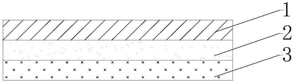
[0024] Such as figure 1 As shown, a conductive film, the conductive film includes a substrate film 1, an optical adjustment layer 2 and a conductive layer 3, the substrate film 1 is connected to the optical adjustment layer 2, and the optical adjustment layer 2 is connected to the optical adjustment layer The conductive layer 3 is connected.

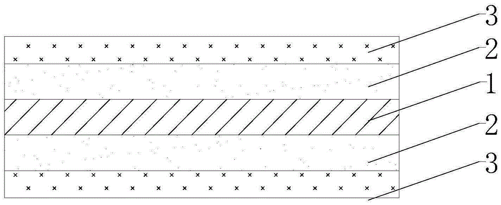
[0025] The conductive film includes two conductive layers 3, two optical adjustment layers 2 are arranged between the two conductive layers 3, and a base film 1 is arranged between the two optical adjustment layers 2.

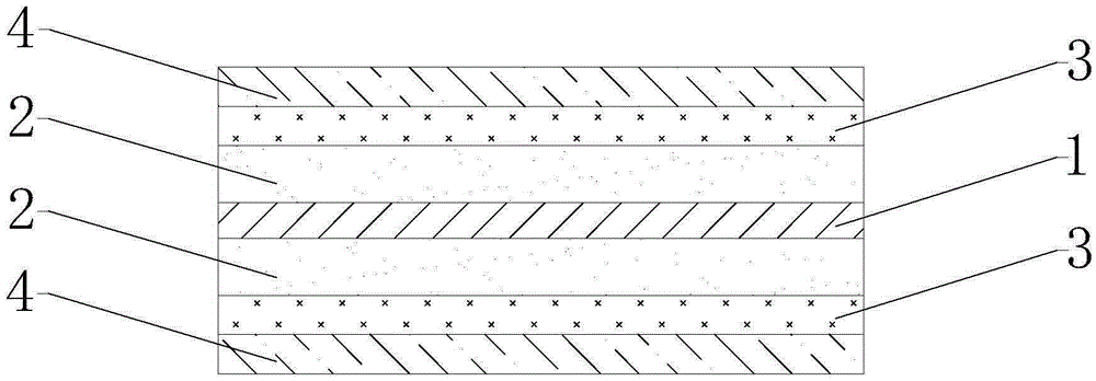
[0026] A layer of flexible transparent film 4 is provided on the outside of the two conductive layers 3 .

[0027] The conductive layer 3 is a graphene mater...


PUM


Abstract

The invention relates to the technical field of electronic information, in particular to a conductive thin film. The conductive thin film comprises a base material thin film, optical adjusting layers and conducting layers, wherein the base material thin film is connected with the optical adjusting layers; the optical adjusting layers are connected with the conducting layers; the conductive thin film comprises two conducting layers; two optical adjusting layers are arranged between the two conducting layers; the base material thin film is arranged between the two optical adjusting layers; flexible transparent thin films are respectively arranged on the outer sides of the two conducting layers; the conducting layers are made of a graphene material; the graphene material is pure graphene; the graphene grows under the conditions of a gas carbon source and a protective gas by a chemical vapor deposition method; and the grown graphene is transferred to the flexible transparent thin films. The conducting layers are conductive organic polymer layers; and a conductive organic polymer compound of each conductive organic polymer layers is one or more of a polythiophene compound, a polyaniline compound or a polypyrrole compound. The conductive thin film has the characteristics of being sensitive in reaction, good in transparency, low in manufacturing cost and the like.

Description

technical field [0001] The invention relates to the technical field of electronic information, in particular to a conductive thin film. Background technique [0002] Touch screen is currently the most simple, convenient and natural way of human-computer interaction. It gives multimedia a new look and is a very attractive new multimedia interactive device. It is mainly used in public information query, automated office, industrial control, military Conducting, electronic games, ordering songs and dishes, multimedia teaching, real estate pre-sales, etc. Transparent electrodes are the core components of touch screens, and transparent electrode technology has therefore become one of the current important research fields. [0003] The current ITO resistive touch screens on the market use the principle of pressure-sensing control. Due to the disadvantage of being fragile, the ITO screen has a very hard surface treatment, so when the user uses it, it often feels unresponsive becau...

Claims


Application Information

Patent Timeline
Patent Type & Authority Applications(China)
IPC IPC(8): H01B5/14G06F3/044
Inventor 黄云鸿
Owner 黄云鸿
Why Eureka
Try Eureka