
Eureka
For R&D, Eureka makes reading and utilizing patents & technical documents easy.
Eureka AIR
Designed for self-driven R&D workflows. Generate viable solutions, solve complex R&D challenges, empower your innovation with AI.

Eureka Materials
Designed for material experts only. Revolutionize your material R&D, from search, analyze, to developing new materials.

TechResearch
Generate reliable direction feasibility study reports for your R&D in just a few steps.

TechSeek
Discover and master advanced knowledge NOW. Basics, ideas, possibilities, all at once.

TechMind
As an expert in R&D Theories, TechMind can generates customized viable solutions instantly.

TechRisk
Analyze your overall solution with one click, know your potential R&D risks in advance.

TechMonitor
Get weekly tech updates, stay abreast of the latest tech innovations and key insights.
Touch panel, manufacturing method thereof, and touch device
A technology of touch panel and touch line, which is applied in the direction of instruments, computing, electrical digital data processing, etc., can solve the problem of poor touch effect of touch panel, and achieve the effect of reducing the influence of touch effect
- Summary
- Abstract
- Description
- Claims
- Application Information
AI Technical Summary
Problems solved by technology
Method used
Image

Examples
Embodiment Construction
[0051] In order to make the object, technical solution and advantages of the present invention clearer, the implementation manner of the present invention will be further described in detail below in conjunction with the accompanying drawings.
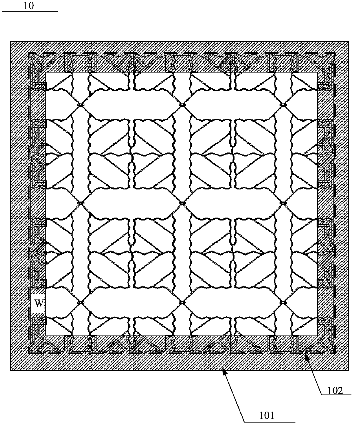
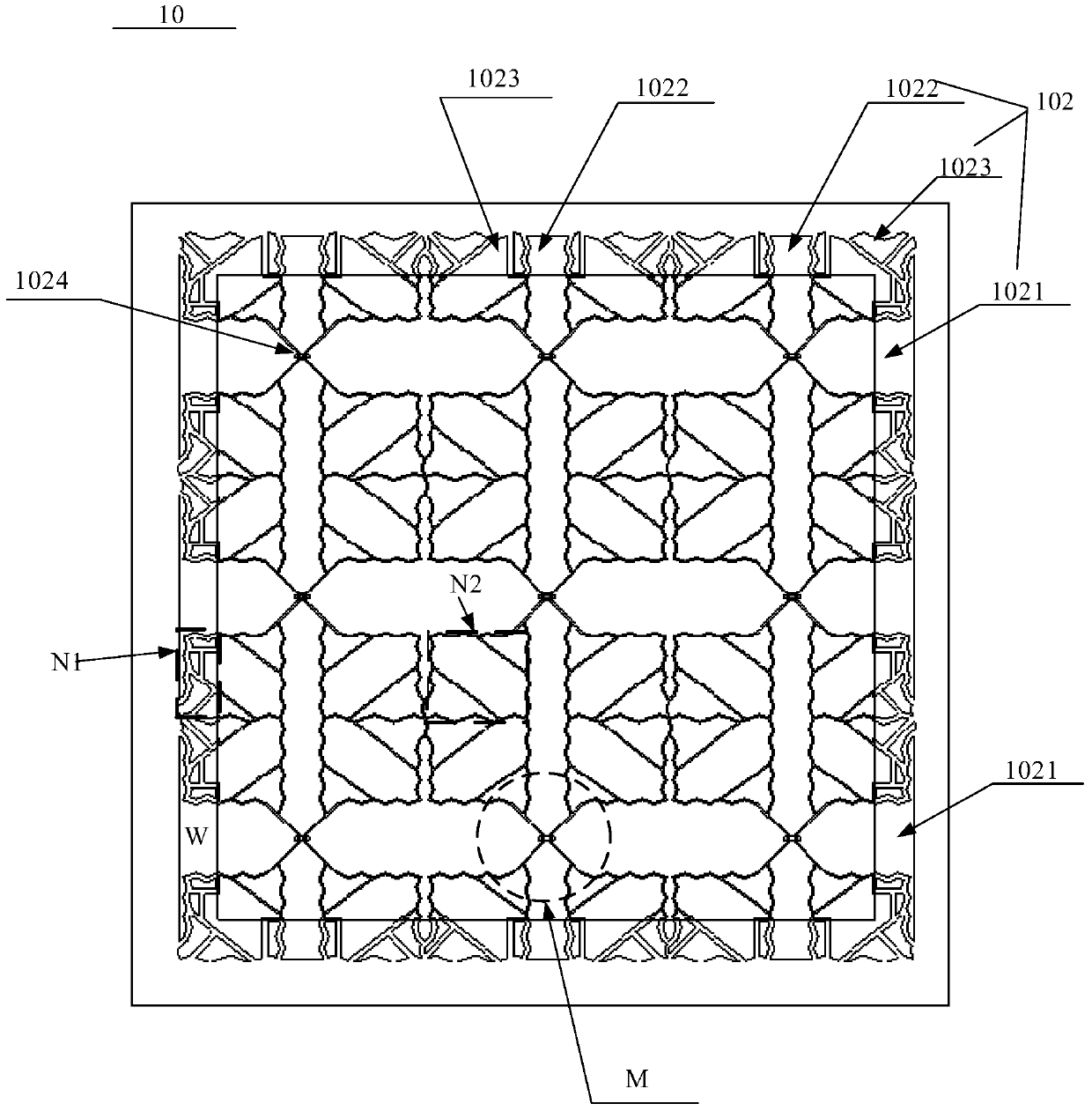
[0052] Such as Picture 1-1 as shown, Picture 1-1 It is a schematic structural diagram of a touch panel 10 provided by an embodiment of the present invention. The touch panel 10 includes:
[0053] Substrate substrate ( Picture 1-1 Not marked in ), the base substrate can be transparent glass.
[0054] A BM101 is formed on the base substrate, and the BM101 is located in an annular area ( Picture 1-1 shaded area in ).
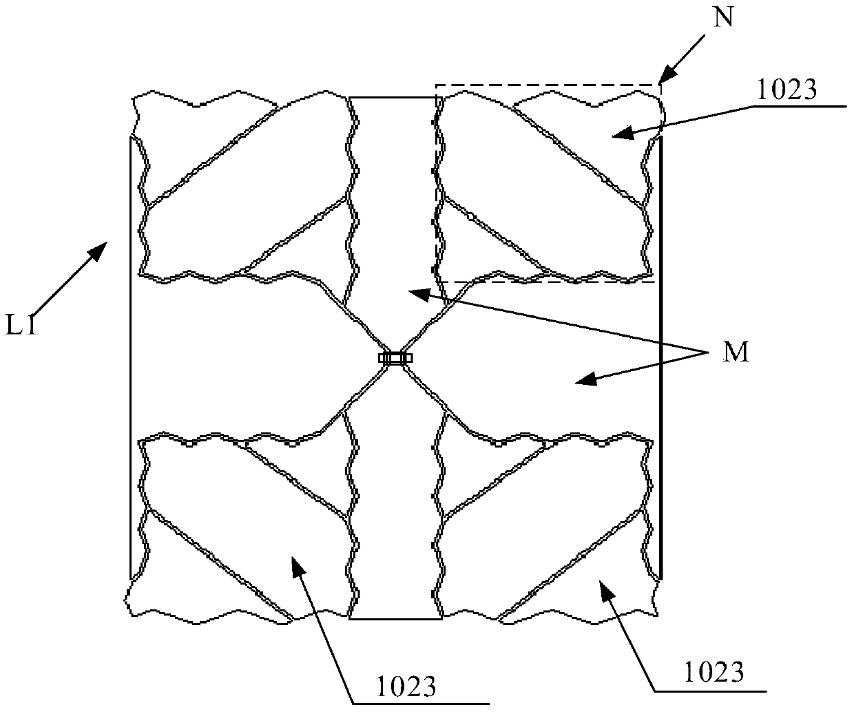
[0055] A transparent conductive pattern 102 ( Picture 1-1 The figure in the dotted line box), there is an overlapping area W between the outer edge of the transparent conductive pattern 102 and the inner edge of the BM, for a clearer description, as Figure 1-2 as shown, Figure 1-2 for Picture 1-1 The structural sc...
PUM
 Abstract
Description
Claims
Application Information
 - R&D Engineer
- R&D Manager
- IP Professional
- Industry Leading Data Capabilities
- Powerful AI technology
- Patent DNA Extraction
Browse by: Latest US Patents, China's latest patents, Technical Efficacy Thesaurus, Application Domain, Technology Topic, Popular Technical Reports.
© 2024 PatSnap. All rights reserved.Legal|Privacy policy|Modern Slavery Act Transparency Statement|Sitemap|About US| Contact US: help@patsnap.com