Memories with sub-block erase architecture
A memory and block technology, applied in static memory, read-only memory, information storage, etc., can solve the problem of consuming memory cell cycle tolerance and other issues
- Summary
- Abstract
- Description
- Claims
- Application Information
AI Technical Summary
Problems solved by technology
Method used
Image

Examples
Embodiment Construction
[0144] In order to make the object, technical solution and advantages of the present invention clearer, the present invention will be described in further detail below in conjunction with specific embodiments and with reference to the accompanying drawings.
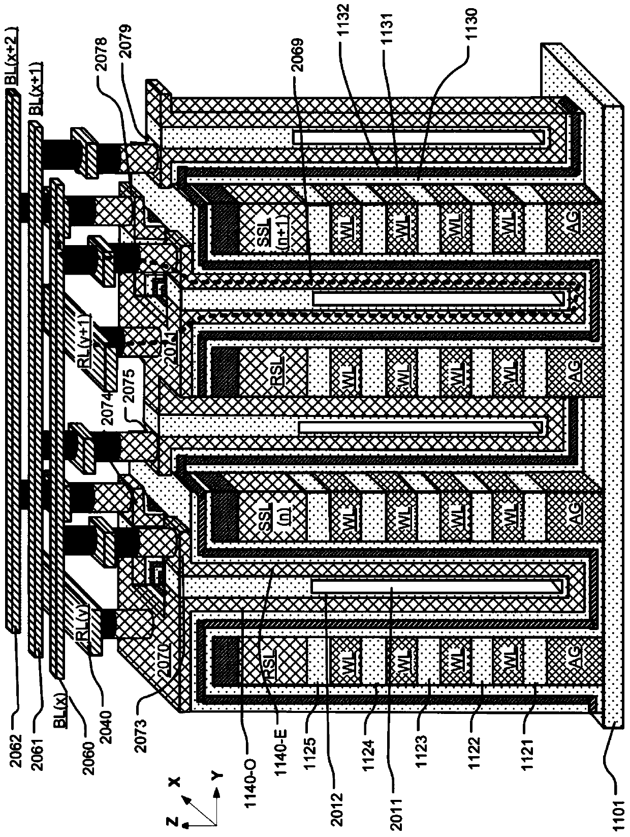
[0145] figure 1 is a schematic diagram of 3D NAND memory, as described in detail in commonly owned and co-pending U.S. Patent Application Serial No. 14 / 637,204, entitled "U-Shaped Vertical Thin-Channel Memory," filed March 03, 2015, which is incorporated Instructions here.
[0146] figure 1 A memory device is shown in which multiple stacks of conductive strips are interleaved with isolation layers 1121 - 1125 and disposed on an isolation substrate 1101 . These stacks are separated by different trenches. The conductive strips of the first and second stacks have sidewalls on first and second sides of the groove separating the stacks. Data storage structures comprising storage layers are formed on the sidewalls o...
PUM
 Abstract
Description
Claims
Application Information
 - R&D
- Intellectual Property
- Life Sciences
- Materials
- Tech Scout
- Unparalleled Data Quality
- Higher Quality Content
- 60% Fewer Hallucinations
Browse by: Latest US Patents, China's latest patents, Technical Efficacy Thesaurus, Application Domain, Technology Topic, Popular Technical Reports.
© 2025 PatSnap. All rights reserved.Legal|Privacy policy|Modern Slavery Act Transparency Statement|Sitemap|About US| Contact US: help@patsnap.com