Transparent solar LED panel

A technology of solar panels and solar energy, applied in electrical components, electric solid state devices, circuits, etc., can solve the problems of inability to install electronic components at the same time, and inability to realize automatic LED power supply.

Pending Publication Date: 2017-05-31
GUANGZHOU QIHONG ELECTRONICS TECH
View PDF5 Cites 2 Cited by
  • Summary
  • Abstract
  • Description
  • Claims
  • Application Information

AI Technical Summary

Problems solved by technology

It is an innovative attempt to apply solar energy to transparent circuit boards and LEDs. The traditional LED substrates are aluminum plates or copper plates, which are opaque. Since electronic components and solar panels cannot be installed on one surface of the LED substrate at the same time, it is impossible to realize LED. Automatic power supply, and through the transparent circuit board, the solar panel can be set on one side, and the electronic components can be set on the other side, and the electronic components will not block the absorption of solar energy by the solar panel, but the setting of this structure is harmful to the ITO conductive film layer, other materials and Bonding welding, packaging, die bonding, dispensing, and energy supply all put forward higher requirements

Method used


Image

  • Transparent solar LED panel

Examples


Embodiment Construction

[0015] The specific embodiments of the present invention will be further described below in conjunction with the accompanying drawings. It should be noted here that the descriptions of these embodiments are used to help understand the present invention, but are not intended to limit the present invention. In addition, the technical features involved in the various embodiments of the present invention described below may be combined with each other as long as they do not constitute a conflict with each other.

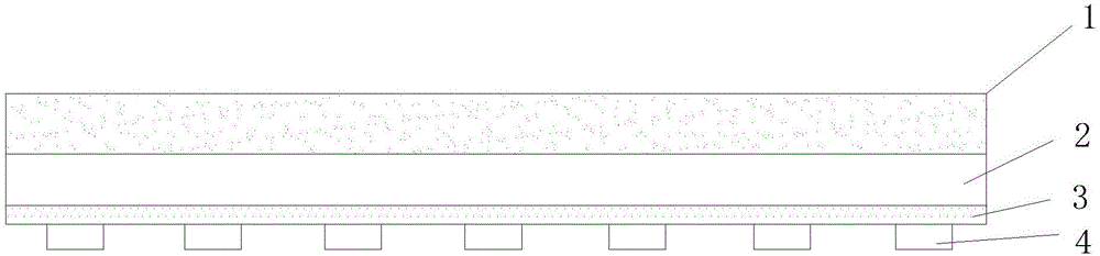
[0016] A transparent solar LED panel, comprising a glass substrate 2, an ITO conductive thin film layer 3, an LED chip 4 and a solar battery panel 1, the ITO conductive thin film layer is formed on the front of the glass substrate by magnetron sputtering, and the thickness of the glass substrate is 0.4 ~ 1.3mm, when preparing the ITO conductive film layer, after washing with deionized water and ultrasonic cleaning, after entering the vacuum chamber, sputter SiO 2 layer,...


PUM

PropertyMeasurementUnit
Thicknessaaaaaaaaaa
Thicknessaaaaaaaaaa
Viscosityaaaaaaaaaa

Abstract

The invention discloses a transparent solar LED panel. The transparent solar LED panel comprises a glass substrate, an ITO conductive thin-film layer, LED chips and solar cell panels. The ITO conductive thin-film layer is formed on the front face of the glass substrate by the method of magnetron sputtering, the ITO conductive thin-film layer forms a circuit by etching, the circuit is provided with a solid crystal region, the LED chips are installed on the solid crystal region upside down, the LED chips are formed in series connection among one another, the back face of the glass substrate is provided with welding spots, the welding spots and the ITO conductive thin-file layer circuit are connected, the solar cell panels and the welding spots are connected in a welding mode, and the solar cell panels are laminated and bonded with the back face of the glass substrate through a laminator. Through the combination of the solar cell panels and the glass substrate, the LED chips are installed on the glass substrate, and on the one hand, the original luminous effect is maintained; on the other hand, the storage of electric energy and a self-powered process can be realized by increasing the storage batteries. The encapsulation requirements are met by controlling the parameters in the magnetron sputtering and controlling the process during encapsulation.

Description

technical field [0001] The invention relates to the field of manufacturing transparent circuit boards, in particular to a transparent solar LED board. Background technique [0002] LED and solar energy have been widely used as a mature technology development, but they are technologies developed based on their respective fields. It is an innovative attempt to apply solar energy to transparent circuit boards and LEDs. The traditional LED substrates are aluminum plates or copper plates, which are opaque. Since electronic components and solar panels cannot be installed on one surface of the LED substrate at the same time, it is impossible to realize LED. Automatic power supply, and through the transparent circuit board, the solar panel can be set on one side, and the electronic components can be set on the other side, and the electronic components will not block the absorption of solar energy by the solar panel, but the setting of this structure is harmful to the ITO conductive ...

Claims


Application Information

Patent Timeline
IPC IPC(8): H01L25/16H01L33/62
CPCH01L25/167H01L33/62H01L2933/0066
Inventor 李天奇
Owner GUANGZHOU QIHONG ELECTRONICS TECH
Why Eureka
Try Eureka