Display panel and preparation method thereof

A technology for display panels and substrates, which is applied in semiconductor/solid-state device manufacturing, semiconductor devices, electrical components, etc., and can solve problems that affect display effects and that heat cannot be discharged reasonably and effectively

Active Publication Date: 2021-04-09
TCL CHINA STAR OPTOELECTRONICS TECH CO LTD
View PDF23 Cites 1 Cited by
  • Summary
  • Abstract
  • Description
  • Claims
  • Application Information

AI Technical Summary

Problems solved by technology

[0005] The purpose of this application is to provide a display panel and its preparation method, which can solve the technical problem that the heat genera

Method used


Image

  • Display panel and preparation method thereof
  • Display panel and preparation method thereof
  • Display panel and preparation method thereof

Examples


Embodiment 1

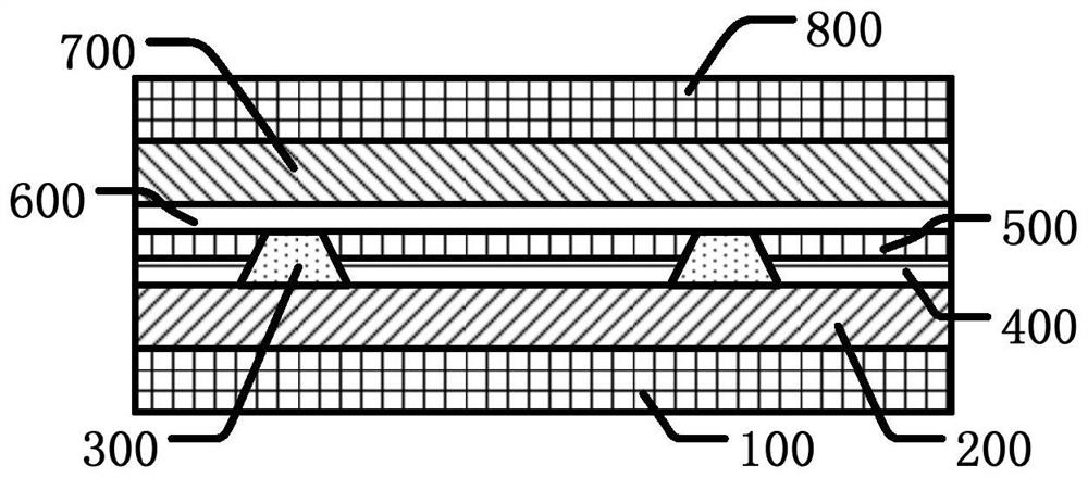
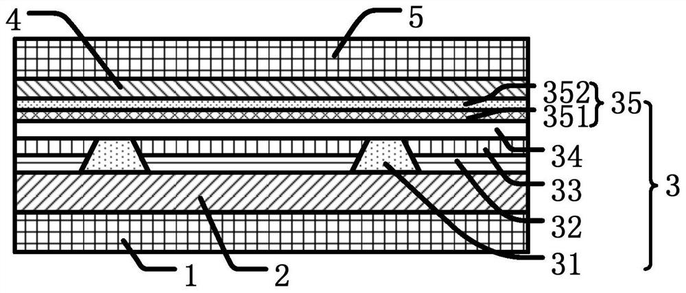
[0034] like figure 2 As shown, this embodiment provides a display panel, including: a substrate 1 , an anode layer 2 , a light emitting and heat dissipation structure 3 , a cathode layer and a cover plate 5 .

[0035] The substrate 1 is generally an array substrate, and the array substrate includes a base substrate, a thin film transistor, an insulating film layer, etc., which will not be described in detail here.

[0036] The anode layer 2 is arranged on the upper surface of the substrate 1, and the material of the anode layer 2 is generally a metal material, which has good electrical conductivity and performance. The anode layer 2 is used to provide circuit support for the light-emitting heat dissipation layer 3 .

[0037] The light-emitting and heat-dissipating structure 3 is arranged on the upper surface of the anode layer 2 to realize the light-emitting function and have a good heat-dissipating effect. The light-emitting heat dissipation layer 3 includes a pixel defini...

Embodiment 2

[0068] like Figure 6 As shown, this embodiment provides a display panel, including: a substrate 1 , an anode layer 2 , a light emitting and heat dissipation structure 3 , a cathode layer and a cover plate 5 .

[0069] The substrate 1 is generally an array substrate, and the array substrate includes a base substrate, a thin film transistor, an insulating film layer, etc., which will not be described in detail here.

[0070] The anode layer 2 is arranged on the upper surface of the substrate 1, and the material of the anode layer 2 is generally a metal material, which has good electrical conductivity and performance. The anode layer 2 is used to provide circuit support for the light-emitting heat dissipation layer 3 .

[0071] The light-emitting and heat-dissipating structure 3 is arranged on the upper surface of the anode layer 2 to realize the light-emitting function and have a good heat-dissipating effect. The light emitting and heat dissipation layer 3 includes a heat dis...


PUM


Abstract

The invention discloses a display panel and a preparation method thereof. The display panel comprises a substrate, an anode layer, a light-emitting heat dissipation structure, a cathode layer and a cover plate; the light-emitting heat dissipation structure comprises a light-emitting layer and a heat dissipation layer; and the heat dissipation layer is located between the light-emitting layer and the cathode layer or the anode layer. The heat dissipation layer can reasonably and effectively dissipate heat generated in the light-emitting process, the light-emitting layer is protected, and the light-emitting effect of the display panel is improved.

Description

technical field [0001] The present application relates to the display field, in particular to a display panel and a preparation method thereof. Background technique [0002] In the working process of the OLED device, the electrodes are energized to form carriers, and the carriers move and jump to the light-emitting layer to recombine to generate excitons, and the excitons excite the light-emitting materials to emit light. [0003] like figure 1 As shown, a common OLED device structure is a substrate 100 , an anode layer 200 , a pixel definition layer 300 , a first auxiliary transport layer 400 , a light emitting layer 500 , a second auxiliary transport layer 600 , a cathode layer 700 and a cover plate 800 . [0004] During the process of emitting light, the OLED device will generate heat, which has a significant impact on the life and performance of the OLED device. Therefore, a reasonable structure is required to realize the heat barrier or rapid dissipation of the OLED de...

Claims


Application Information

Patent Timeline
IPC IPC(8): H01L51/52H01L27/32H01L51/56
CPCH10K59/12H10K50/85H10K50/87H10K71/00
Inventor 宋媛媛
Owner TCL CHINA STAR OPTOELECTRONICS TECH CO LTD
Why Eureka
Try Eureka