A kind of oled pixel circuit and method for slowing down aging of oled device

A technology of pixel circuit and power supply, which can be applied to instruments, static indicators, etc., and can solve problems such as light-emitting diodes are prone to aging

Active Publication Date: 2019-08-13
SHENZHEN CHINA STAR OPTOELECTRONICS SEMICON DISPLAY TECH CO LTD
View PDF8 Cites 0 Cited by
  • Summary
  • Abstract
  • Description
  • Claims
  • Application Information

AI Technical Summary

Problems solved by technology

[0005] The purpose of the present invention is to provide an OLED pixel circuit and a method for slowing down the aging of OLED devices, so as to solve the problem that the light-emitting diodes in the existing OLED pixel circuit are prone to aging under DC bias for a long time

Method used


Image

  • A kind of oled pixel circuit and method for slowing down aging of oled device
  • A kind of oled pixel circuit and method for slowing down aging of oled device
  • A kind of oled pixel circuit and method for slowing down aging of oled device

Examples


Embodiment Construction

[0064] In order to further illustrate the technical means adopted by the present invention and its effects, the following describes in detail in conjunction with preferred embodiments of the present invention and accompanying drawings. Apparently, the described embodiments are only some of the embodiments of the present invention, but not all of them. Based on the embodiments of the present invention, all other embodiments obtained by persons of ordinary skill in the art without creative efforts fall within the protection scope of the present invention.

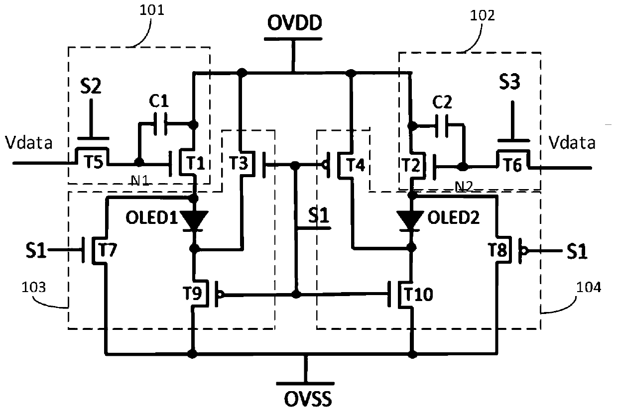
[0065] see figure 2 , the present invention provides an OLED pixel circuit, the OLED pixel circuit includes: a first sub-pixel driving unit 101, a second sub-pixel driving unit 102, a first reverse bias unit 103, and a second reverse bias unit 104 ; Wherein, the first sub-pixel driving unit 101 includes: the first thin film transistor T1, the fifth thin film transistor T5, the first capacitor C1 and the first light emitting...


PUM


Abstract

The invention provides an OLED pixel circuit and a method for slowing down the aging of OLED devices. The OLED pixel circuit and the method for slowing down the aging of the OLED device are provided with a first sub-pixel driving unit, a second sub-pixel driving unit, a first reverse bias unit, and a second reverse bias unit, and with simple control timing, The first light emitting diode and the second light emitting diode are not always in the DC bias state, and the first light emitting diode and the second light emitting diode alternately emit light during different frames, reducing the light emission of the first light emitting diode and the second light emitting diode time, the aging of the first light-emitting diode and the second light-emitting diode is slowed down, and the display quality of the panel is improved.

Description

technical field [0001] The invention relates to the field of display technology, in particular to an OLED pixel circuit and a method for slowing down the aging of OLED devices. Background technique [0002] The active matrix light emitting diode (Active Matrix Organic Light Emitting Diode, AMOLED) can emit light by driving the current generated by the thin film transistor (Thin Film Transistor, TFT) in the saturated state. The traditional AMOLED pixel circuit is often a 2T1C driving circuit. see figure 1 , the 2T1C circuit includes two TFTs and a capacitor (Capacitor), wherein, T1 is the drive tube of the pixel circuit, T2 is the switch tube, the scan line Gate turns on the switch tube T2, the data voltage Vdata charges the storage capacitor Cst, and the switch is switched during the light emitting period. The tube T2 is turned off, and the voltage stored on the capacitor keeps the driving tube T1 turned on, and the conduction current makes the light-emitting diode OLED emi...

Claims


Application Information

Patent Timeline
Patent Type & Authority Patents(China)
IPC IPC(8): G09G3/3225
CPCG09G3/3225G09G2320/043G09G2300/0443G09G3/3233G09G2300/0861G09G2310/0262
Inventor 常勃彪陈小龙温亦谦
Owner SHENZHEN CHINA STAR OPTOELECTRONICS SEMICON DISPLAY TECH CO LTD
Why Eureka
Try Eureka