Optical path control structure, pixel structure and preparation method thereof, and display panel

A technology for controlling structure and pixel structure, which is applied in circuits, semiconductor/solid-state device manufacturing, diodes, etc., can solve the problems of difficult process, difficult realization, high power consumption, etc., and achieve the goal of expanding viewing angle, meeting performance requirements, and realizing thickness reduction Effect

Active Publication Date: 2018-09-14
BOE TECH GRP CO LTD
View PDF5 Cites 10 Cited by
  • Summary
  • Abstract
  • Description
  • Claims
  • Application Information

AI Technical Summary

Problems solved by technology

At present, the application of quantum dot technology in the display field mainly includes the following two types: one is to use quantum dot technology in the backlight of liquid crystal display, but it fails to make good use of the advantages of quantum dots, and it also brings power consumption. high and high cost; the other is to replace the color film layer with a quantum dot material layer, and realize color display through light and color conversion, but when using a quantum dot material layer to replace the color film layer, a built-in polarizer is required. The process is difficult, so it is difficult to realize

Method used


Image

  • Optical path control structure, pixel structure and preparation method thereof, and display panel
  • Optical path control structure, pixel structure and preparation method thereof, and display panel
  • Optical path control structure, pixel structure and preparation method thereof, and display panel

Examples


Embodiment Construction

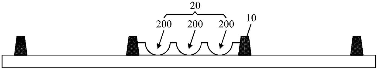
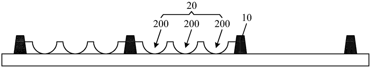
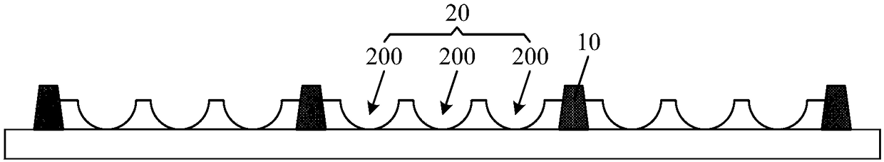
[0031] Example embodiments will now be described more fully with reference to the accompanying drawings. Example embodiments may, however, be embodied in many forms and should not be construed as limited to the examples set forth herein; rather, these embodiments are provided so that this disclosure will be thorough and complete and will fully convey the concept of example embodiments to those skilled in the art. The described features, structures, or characteristics may be combined in any suitable manner in one or more embodiments.

[0032] Furthermore, the drawings are merely schematic illustrations of the present disclosure and are not necessarily drawn to scale. The same reference numerals in the drawings denote the same or similar parts, and thus repeated descriptions thereof will be omitted. Some of the block diagrams shown in the drawings are functional entities and do not necessarily correspond to physically or logically separate entities. These functional entities ...


PUM


Abstract

The present invention provides an optical path control structure, a pixel structure and a preparation method thereof, and a display panel, and relates to the technical field of display. The optical control structure comprises a pixel definition layer and a plurality of optical path control units located in an area limited by the pixel definition layer, the at least one optical path control unit inthe plurality of optical path control units comprises a scattering unit, and the scattering unit comprises one or more than one scattering lens, and the scattering lens is configured to perform scattering of incident light. The optical path control structure, the pixel structure and the preparation method thereof, and the display panel can ensure the optical distance of light in the quantum dot layer while reducing the thickness of the quantum dot layer.

Description

technical field [0001] The present disclosure relates to the field of display technology, and in particular to an optical path control structure, a pixel structure and a manufacturing method thereof, and a display panel. Background technique [0002] The quantum dot (Quantum Dot, QD) display device has the advantage of a wide color gamut, because it can realize the modulation of the emission spectrum according to the particle size of the quantum dot material, so the color spectrum is more continuous. At present, the application of quantum dot technology in the display field mainly includes the following two types: one is to use quantum dot technology in the backlight of liquid crystal display, but it fails to make good use of the advantages of quantum dots, and it also brings power consumption. The disadvantages of high cost and high cost; the other is to replace the color film layer with a quantum dot material layer, and realize color display through light and color convers...

Claims


Application Information

Patent Timeline
Patent Type & Authority Applications(China)
IPC IPC(8): H01L27/15H01L33/50H01L33/58H01L27/32H01L51/56
CPCH01L27/156H01L33/505H01L33/507H01L33/508H01L33/58H01L2933/0058H01L2933/0041H10K59/38H10K59/50H10K71/00
Inventor 赵德江郝运
Owner BOE TECH GRP CO LTD
Why Eureka
Try Eureka