An erasing method of a flash memory device and a flash memory device

A technology of flash memory and registers, which is applied to the erasing method of flash memory and the field of flash memory, can solve the problems of low erasing efficiency, achieve the effects of prolonging service life, reducing the number of erasing pulses, and improving erasing efficiency

Inactive Publication Date: 2019-01-22
YANGTZE MEMORY TECH CO LTD
View PDF5 Cites 5 Cited by
  • Summary
  • Abstract
  • Description
  • Claims
  • Application Information

AI Technical Summary

Problems solved by technology

[0003] In related technologies, when performing an erasing operation on NAND, it is often necessary to adjust the erasing voltage multiple times and generate multiple erasing pulses to successfully erase, and the erasing efficiency is low.

Method used


Image

  • An erasing method of a flash memory device and a flash memory device
  • An erasing method of a flash memory device and a flash memory device
  • An erasing method of a flash memory device and a flash memory device

Examples


Embodiment Construction

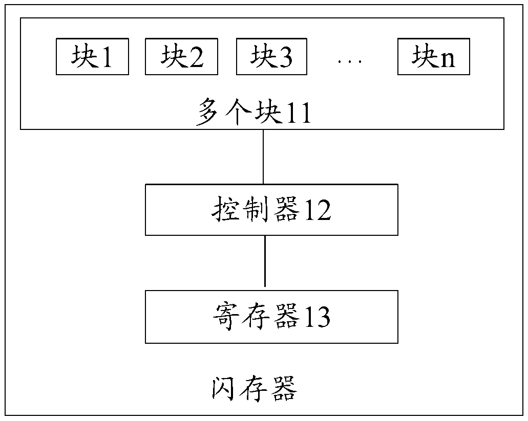
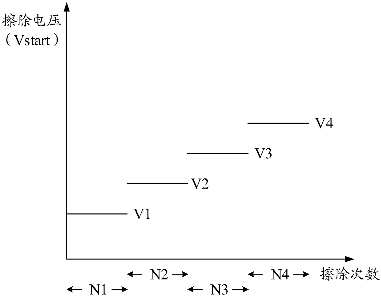
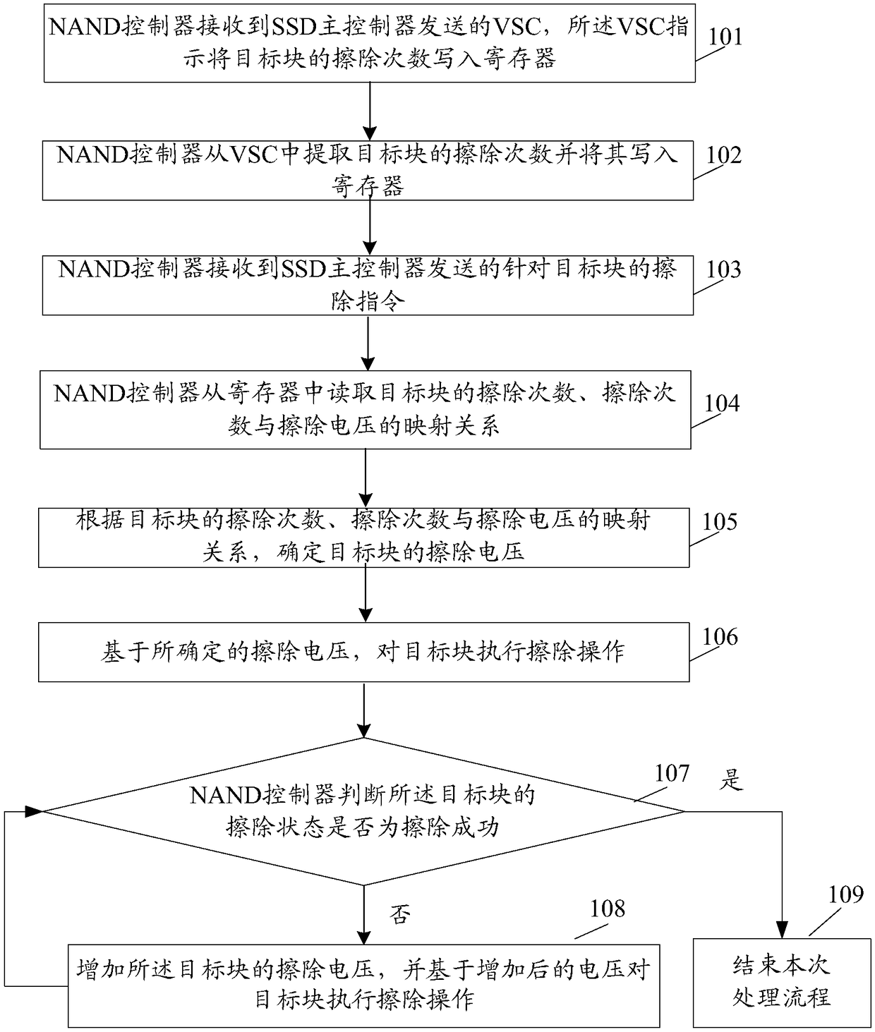
[0058] The present invention will be described in further detail below in conjunction with the accompanying drawings and embodiments. It should be understood that the examples provided here are only used to explain the present invention, not to limit the present invention. In addition, the examples provided below are some examples for implementing the present invention, rather than providing all the examples for implementing the present invention. In the case of no conflict, the technical solutions recorded in the embodiments of the present invention can be combined in any manner implement.

[0059] It should be noted that, in the embodiments of the present invention, the terms "comprising", "comprising" or any other variant thereof are intended to cover a non-exclusive inclusion, so that a method or device comprising a series of elements not only includes the explicitly stated elements, but also include other elements not explicitly listed, or also include elements inherent ...


PUM


Abstract

The invention discloses an erasing method of a flash memory device and a flash memory device. The flash memory device comprises a plurality of blocks, each of which is composed of a plurality of memory cells, wherein the memory cells are the smallest data storage units of the flash memory device; a controller, configured to receive a write instruction carrying an erase parameter from an external main controller, and write the erase parameter into a register, and to receive an erase instruction for a target block from an external master controller and obtain an erase parameter of the target block, determine an erase voltage corresponding to the target block based on an erase parameter of the target block, and perform an erase operation on the target block based on the determined erase voltage; and a register which is used for storing the erase parameter.

Description

technical field [0001] The invention relates to the technical field of semiconductors, in particular to a method for erasing a flash memory and the flash memory. Background technique [0002] In NAND flash memory, P (Program) / E (Erase) Cycle, called erasing cycle (number of times), is a key parameter for judging the life of NAND flash memory. With the increase of P / E Cycle, the oxide layer between the floating gate and the channel is worn more and more seriously, which makes it more and more difficult to control the electrons in the floating gate. The final result is that the life of NAND has come to an end. Therefore, reducing the P / E cycle is the main way to extend the life of NAND. [0003] In related technologies, when performing an erasing operation on NAND, it is often necessary to adjust the erasing voltage multiple times and generate multiple erasing pulses to successfully erasing, and the erasing efficiency is low. Contents of the invention [0004] In order to ...

Claims


Application Information

Patent Timeline
Patent Type & Authority Applications(China)
IPC IPC(8): G11C16/16G11C16/34
CPCG11C16/16G11C16/3495
Inventor 梁轲李跃平侯春源
Owner YANGTZE MEMORY TECH CO LTD
Why Eureka
Try Eureka