OLED substrate and transparent display

A technology of substrate and transparent area, which is applied in the manufacture of electric solid-state devices, semiconductor devices, and semiconductor/solid-state devices, etc., can solve the problems of low light transmittance of transparent displays, so as to improve light transmittance, improve image brightness, and improve The effect of user experience

Active Publication Date: 2019-02-01
BOE TECH GRP CO LTD
View PDF11 Cites 24 Cited by
  • Summary
  • Abstract
  • Description
  • Claims
  • Application Information

AI Technical Summary

Problems solved by technology

[0004] Embodiments of the present invention provide an OLED substrate and a transparent display, which can solve the problem of low light transmittance of the transparent display

Method used


Image

  • OLED substrate and transparent display
  • OLED substrate and transparent display
  • OLED substrate and transparent display

Examples


Embodiment Construction

[0034] The following will clearly and completely describe the technical solutions in the embodiments of the present invention with reference to the accompanying drawings in the embodiments of the present invention. Obviously, the described embodiments are only some, not all, embodiments of the present invention. Based on the embodiments of the present invention, all other embodiments obtained by persons of ordinary skill in the art without making creative efforts belong to the protection scope of the present invention.

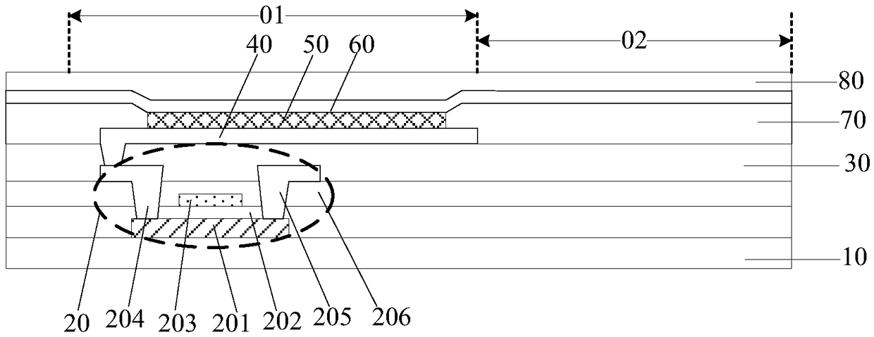
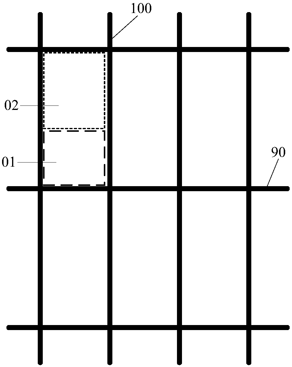
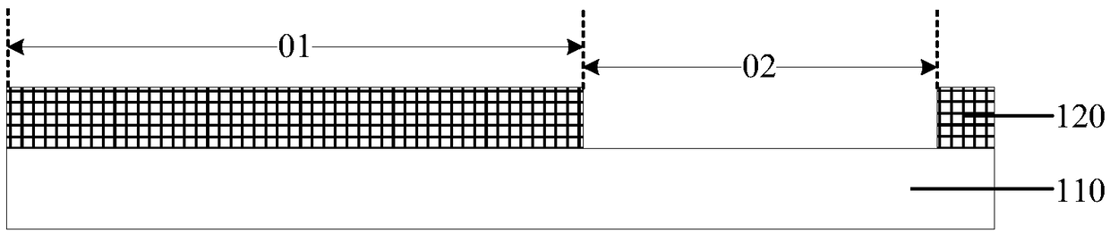
[0035] In the related art, a transparent organic light emitting display (Organic Light Emitting Display, OLED for short) includes an OLED substrate, and the OLED substrate includes a light-emitting area and a transparent area. The transparent area in the OLED substrate can be designed in the OLED substrate as required, for example, it can be as follows figure 2 The gate lines 90 and data lines 100 intersecting horizontally and vertically are shown as a plural...


PUM


Abstract

The embodiment of the invention provides an OLED substrate and a transparent display, and relates to the technical field of display. The problem can be solved that the light transmission of the display is low. The OLED substrate comprises a luminous area and a transparent area. The OLED substrate comprises a substrate and a display layer arranged on the substrate, wherein the portion of the display layer is located on the transmission area has a first hollow area. The OLED substrate and the transparent display are configured to improve the light transmission of the transparent display.

Description

technical field [0001] The invention relates to the field of display technology, in particular to an OLED substrate and a transparent display. Background technique [0002] With the rapid development of science and technology, various new technologies continue to emerge, among which transparent displays have attracted more and more attention due to their unique properties. [0003] A transparent display means that the display itself has a certain degree of light penetration, such as figure 1 As shown, the transparent display includes both a light-emitting area 01 and a transparent area 02 . Among them, an important index determining the performance of the transparent display panel is the transmittance of the transparent area 02, which determines the amount of light transmitted through the display panel and affects the brightness of the image obtained through the transparent area 02. However, if figure 1 As shown, since the film layers of the transparent display such as th...

Claims


Application Information

Patent Timeline
Patent Type & Authority Applications(China)
IPC IPC(8): H01L27/32H01L51/52
CPCH10K59/12H10K50/85H10K59/121H10K59/126H10K59/122H10K59/131
Inventor 王和金谢明哲王品凡
Owner BOE TECH GRP CO LTD
Why Eureka
Try Eureka