A kind of optocoupler and preparation method thereof

A photoelectric coupler and photocurrent technology, applied in circuits, electrical components, semiconductor devices, etc., can solve problems such as difficult to achieve high-speed response, and achieve the effects of improving light absorption efficiency, reducing volume, and compatible manufacturing processes

Active Publication Date: 2021-02-12
UNIV OF ELECTRONICS SCI & TECH OF CHINA
View PDF0 Cites 0 Cited by
  • Summary
  • Abstract
  • Description
  • Claims
  • Application Information

AI Technical Summary

Problems solved by technology

Therefore, in the face of the demand for long-wavelength light in practical applications of optocouplers, it is difficult to achieve high-speed response

Method used


Image

  • A kind of optocoupler and preparation method thereof
  • A kind of optocoupler and preparation method thereof
  • A kind of optocoupler and preparation method thereof

Examples


Embodiment Construction

[0036] In order to make the solutions and principles of the present invention more clear to those skilled in the art, the following describes in detail in conjunction with the drawings and specific embodiments.

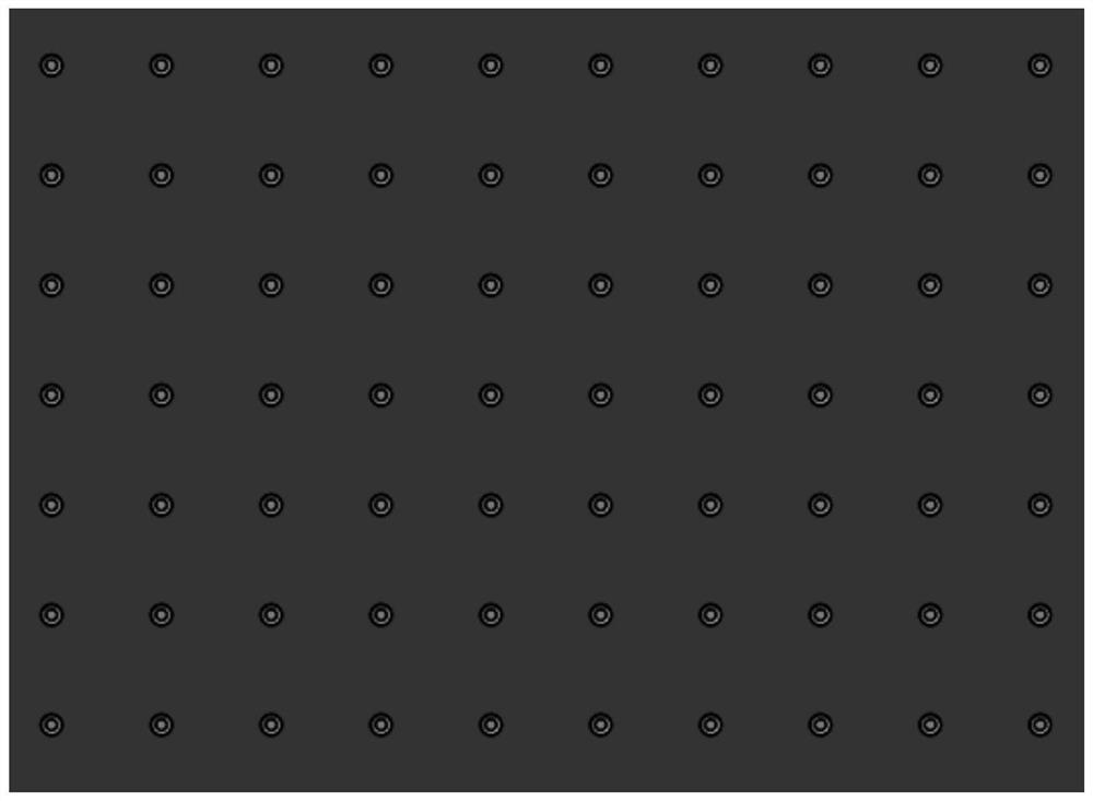
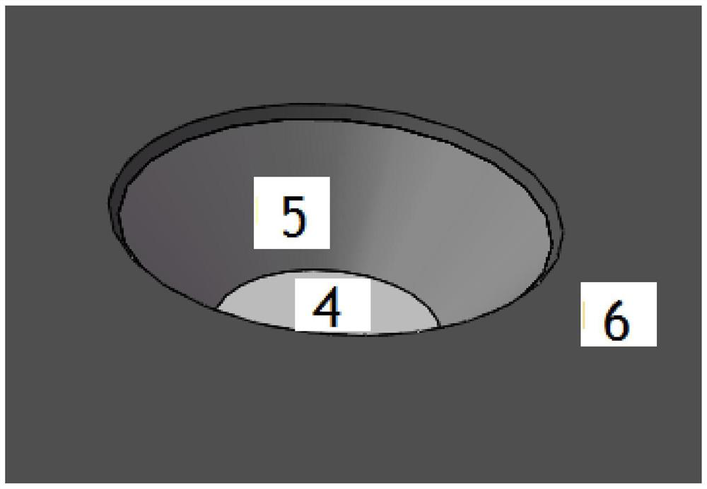
[0037] This embodiment provides an optocoupler, including a light emitting unit and a light receiving unit separated by an isolation region, and a post-processing circuit; the light receiving unit is used to receive the light emitted by the light emitting unit and form a photocurrent. The current is converted into an electrical signal output by the post-processing circuit; as figure 1 As shown, the light receiving unit includes a p-type doped semiconductor layer 4, an intrinsic semiconductor layer 5 and an n-type doped semiconductor layer 6 that are stacked sequentially from bottom to top, as figure 2 and 3 As shown, the n-type doped semiconductor layer 6 runs through the intrinsic semiconductor layer 5 and extends to the surface of the p-type doped semiconductor la...


PUM

PropertyMeasurementUnit
thicknessaaaaaaaaaa
thicknessaaaaaaaaaa

Abstract

An optocoupler and a preparation method thereof belong to the technical field of optoelectronic devices. The photocoupler includes a light-emitting unit, a light-receiving unit, and a post-processing circuit; the light-receiving unit is based on a PIN junction with a micro-nano hole structure, and the pores of the micro-nano hole structure start from the n-type layer through the intrinsic The layer extends to the surface of the p-type layer, and the micro-nano hole structure is periodically arranged to form a photodetection array; the light-receiving unit is arranged above the CMOS integrated circuit to realize monolithic integration. The invention significantly reduces the response time of the light receiving unit, and improves the overall response speed of the photocoupler from the ns level to the ps level. The micro-nano hole array is beneficial to extend the absorption spectrum to a higher wavelength and improve the light absorption efficiency. In addition, the manufacturing process provided by the invention is compatible with the integrated circuit manufacturing process. Compared with the existing photosensitive chip, the device performance is significantly improved while the volume is reduced, the yield and device reliability are improved, and the production cost is also reduced.

Description

technical field [0001] The invention belongs to the technical field of optoelectronic devices, and in particular relates to a single-chip integrated photoelectric coupler with high responsivity and sensitivity and a preparation method thereof. Background technique [0002] With the continuous development of the optoelectronic industry and the wide application of optocoupler technology, the research, design and development of optocouplers (referred to as optocouplers) are becoming more and more important. As a commonly used one-way isolation device, optocouplers are increasingly appearing in high-speed, high-reliability working environments. As the peripheral circuits of optocouplers work at higher and higher speeds, sending means that they need The response time of optocoupler devices is getting shorter and shorter. Otherwise, when the response time of the optocoupler is much smaller than the operating frequency of the peripheral circuit, its response speed will become a "b...

Claims


Application Information

Patent Timeline
Patent Type & Authority Patents(China)
IPC IPC(8): H01L31/12
CPCH01L31/125
Inventor 梁志清赵嘉学罗宗海石锦涛张铭徐灿明郭泽宇刘子骥
Owner UNIV OF ELECTRONICS SCI & TECH OF CHINA
Why Eureka
Try Eureka