

Array substrate, related current detection method, display panel and display device
A technology of array substrate and current detection, applied in circuits, electrical components, electrical solid devices, etc., to achieve the effect of low cost and accurate measurement
- Summary
- Abstract
- Description
- Claims
- Application Information
AI Technical Summary
Problems solved by technology
Method used
Image


Examples
Embodiment Construction
[0031] In order to make the object, technical solution and advantages of the present invention more clear, the specific implementation manners of the array substrate, related current detection method, display panel and display device provided by the embodiments of the present invention will be described in detail below with reference to the accompanying drawings.
[0032] The present invention will be described in detail below in conjunction with specific embodiments. It should be noted that this embodiment is for better explaining the present invention, but not limiting the present invention.
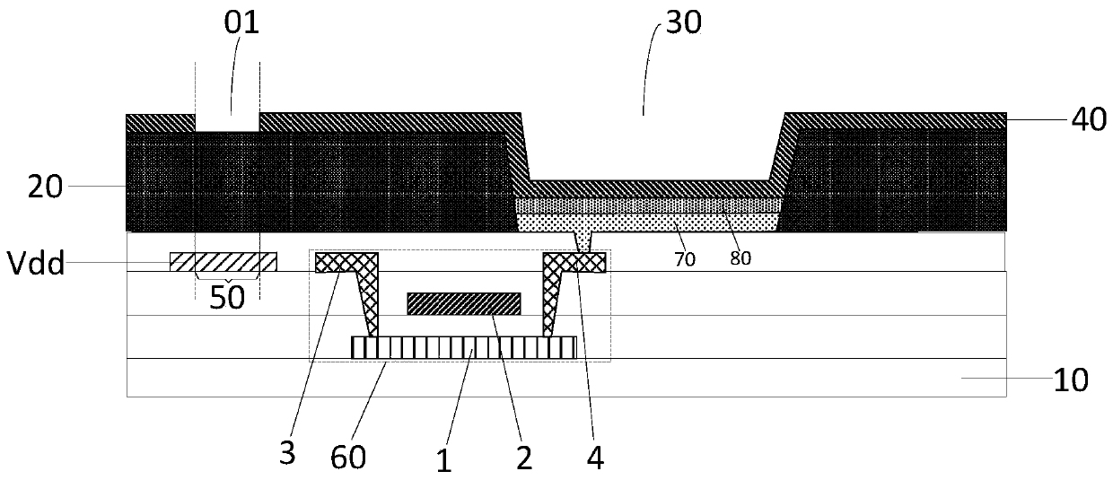
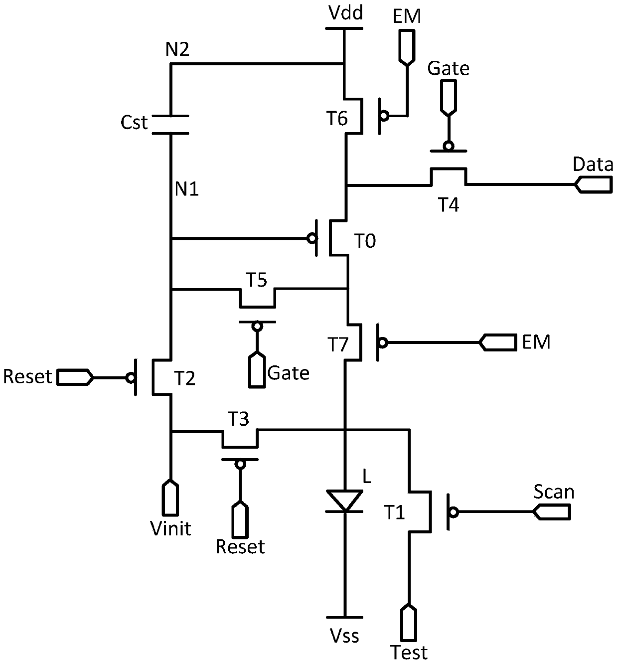
[0033] An array substrate provided by an embodiment of the present invention, such as figure 1 and figure 2 as shown, figure 1 is a schematic cross-sectional structure diagram of some film layers in the array substrate, figure 2 It is a schematic structural diagram of a pixel circuit in the array substrate. The array substrate includes: a base substrate 10, a plurality of pixel ci...
PUM
 Abstract
Description
Claims
Application Information