Array substrate, display device and driving method thereof

A technology for array substrates and display devices, applied in static indicators, instruments, etc., can solve the problems that the gate cannot be fully opened, the pixel charging time is short, and the screen display is uneven, so as to achieve normal display, reduce RC delay, and ensure The effect of charging time

CN110060652AInactive Publication Date: 2019-07-26BEIHAI HKC OPTOELECTRONICS TECH CO LTD +1
14 Cites 10 Cited by

Patent Information

Authority / Receiving Office
CN · China
Current Assignee / Owner
Publication Date
2019-07-26
Estimated Expiration
Not applicable · inactive patent

Smart Images

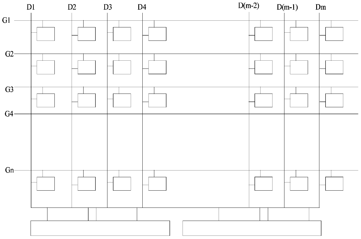
  • Figure 1
    Figure 1
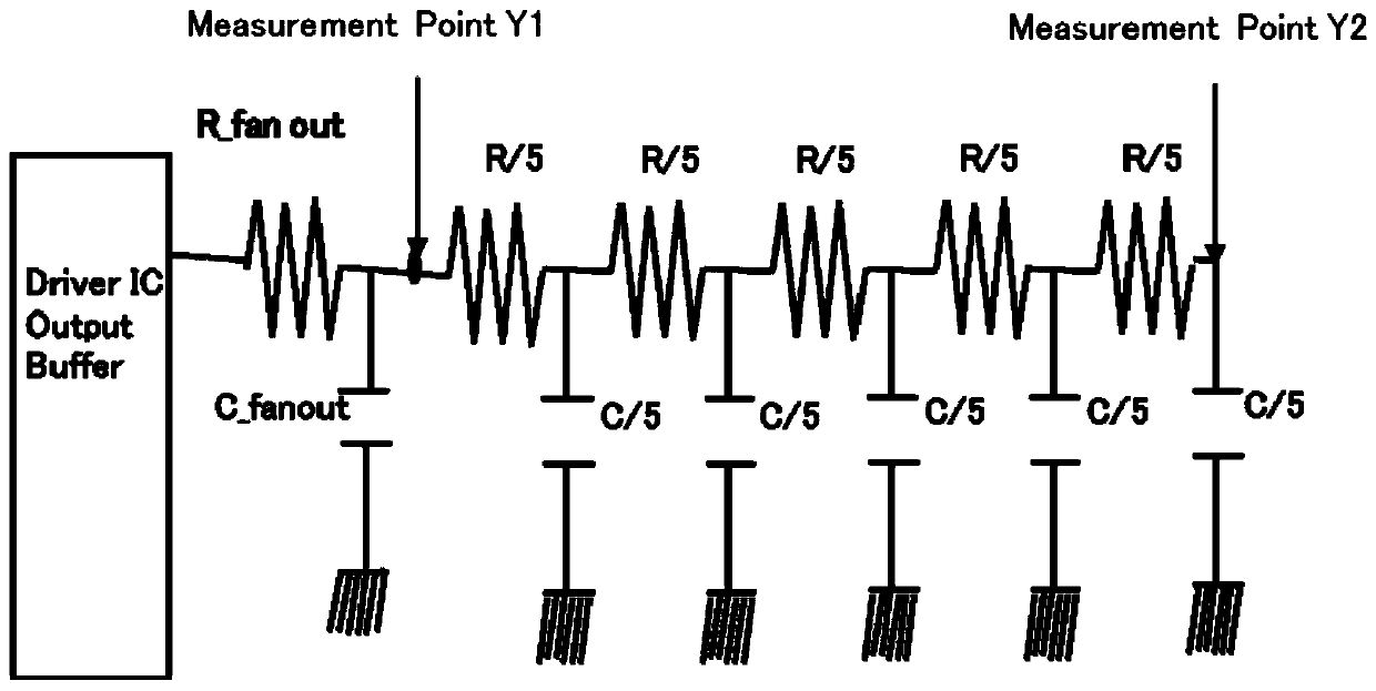
  • Figure 2
    Figure 2
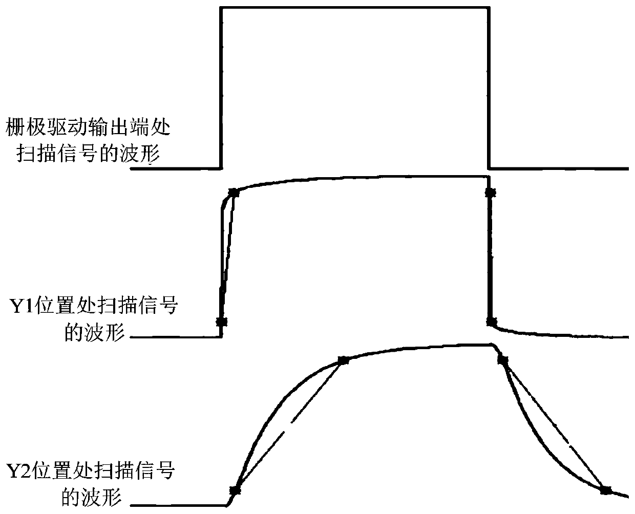
  • Figure 3
    Figure 3
Patent Text Reader

Abstract

The embodiment of the invention provides an array substrate, a display device and a driving methodthereof. The array substrate comprises a substrate, a plurality of scanning lines and a plurality of data lines. The plurality of scanning lines and the plurality of data lines are arranged in a crossed manner to form a plurality of pixel units which are arranged in an array manner. At least one row of pixel units corresponds to two scanning lines, and the two scanning lines corresponding to the same row of pixel units synchronously receive scanning signals. According to the array substrate, the two scanning lines are arranged on the same row of pixel units, the number of the electrically connected pixel units on each scanning line is reduced, then the resistance and capacitance delay on the scanning lines is reduced, and the charging time of the grid electrode is guaranteed. Moreover, the two scanning lines corresponding to the pixel units in the same row synchronously receive scanning signals, so that the grid electrodes of the pixel units in the same row are enabled to be synchronously opened, and the normal display of images is realized.
Need to check novelty before this filing date? Find Prior Art

Description

technical field

[0001] The present invention relates to the technical field of liquid crystal display, in particular to an array substrate display device and a driving method thereof. Background technique

[0002] With the development of TV industry technology, people have higher and higher requirements for the quality of liquid crystal display, and the resolution of liquid crystal display panel is also higher and higher. At present, 4K2K (ie UHD: 3840x2160) TV has become the mainstream of the market, and the market share The resolution is getting higher and higher, and the development of products with a higher resolution of 8K4K (7680x4320) is also in progress.

[0003] There is RC Delay (resistor-capacitance delay) at each position of a scan line, so the gate open states of the pixel units on the same scan line are also different. The RC Delay near the gate drive circuit side is small, and the gate drive The RC delay on the circuit side is large. For an 8K4K LCD panel, t...

Examples

Embodiment Construction

[0024] In order to make the above objects, features and advantages of the present invention more comprehensible, specific implementations of the present invention will be described in detail below in conjunction with the accompanying drawings. In the following description, numerous specific details are set forth in order to provide a thorough understanding of the present invention. However, the present invention can be implemented in many other ways different from those described here, and those skilled in the art can make similar improvements without departing from the connotation of the present invention, so the present invention is not limited by the specific implementations disclosed below.

[0025] Usually the refresh frequency of the liquid crystal display panel is 60Hz, and the turn-on time of each line (that is, the charging time) t=1 / 60 / V total , V total is the total number of scan lines. It can be seen from the above formula that the higher the resolution of the LC...