Mixed-media copper-diffusion-resistant blocking layer for copper interconnection and fabrication method of blocking layer

A barrier layer and copper interconnection technology, which is applied in semiconductor/solid-state device manufacturing, semiconductor/solid-state device components, semiconductor devices, etc., can solve the problem of poor consistency and compactness of the diffusion barrier layer, complex process, and thermal damage of devices, etc. problem, achieve the effect of enhancing anti-diffusion ability, simple and feasible process, and preventing failure

Inactive Publication Date: 2012-12-19
FUDAN UNIV
View PDF5 Cites 15 Cited by
  • Summary
  • Abstract
  • Description
  • Claims
  • Application Information

AI Technical Summary

Problems solved by technology

[0004] At present, the physical vapor deposition (PVD) process is generally used to deposit the diffusion barrier layer. The consistency and compactness of the grown diffusion barrier layer are relatively poor. When exposed to air or oxygen-containing gas, it is easy to be destroyed Moreover, the diffusion barrier layer deposited by the PVD process needs to be thermally annealed to have a good contact after it is prepared, and then annealing will bring thermal damage and negative effects to the fabricated device. After the barrier layer is grown, it is still necessary to deposit a layer of copper seed crystals on the surface before electroplating metal copper, and the process is complicated

Method used


Image

  • Mixed-media copper-diffusion-resistant blocking layer for copper interconnection and fabrication method of blocking layer
  • Mixed-media copper-diffusion-resistant blocking layer for copper interconnection and fabrication method of blocking layer
  • Mixed-media copper-diffusion-resistant blocking layer for copper interconnection and fabrication method of blocking layer

Examples


Embodiment Construction

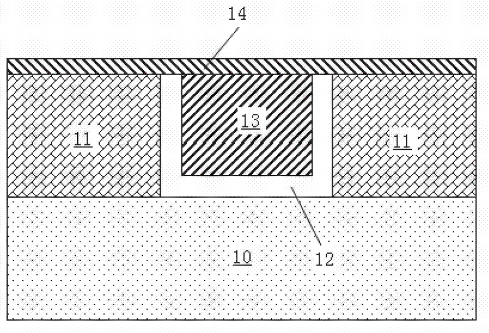
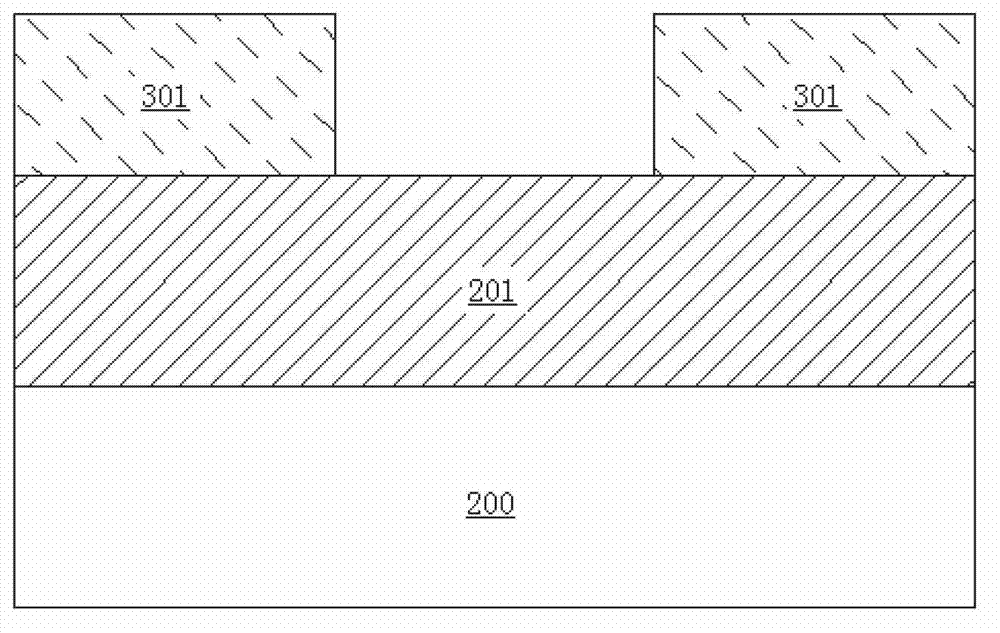
[0028] The present invention will be further described in detail below in conjunction with the accompanying drawings and specific embodiments. In the drawings, for the convenience of illustration, the thicknesses of layers and regions are enlarged or reduced, and the sizes shown do not represent actual sizes. Although these figures do not fully reflect the actual size of the device, they still completely reflect the mutual positions between the regions and the constituent structures, especially the upper-lower and adjacent relationships between the constituent structures.

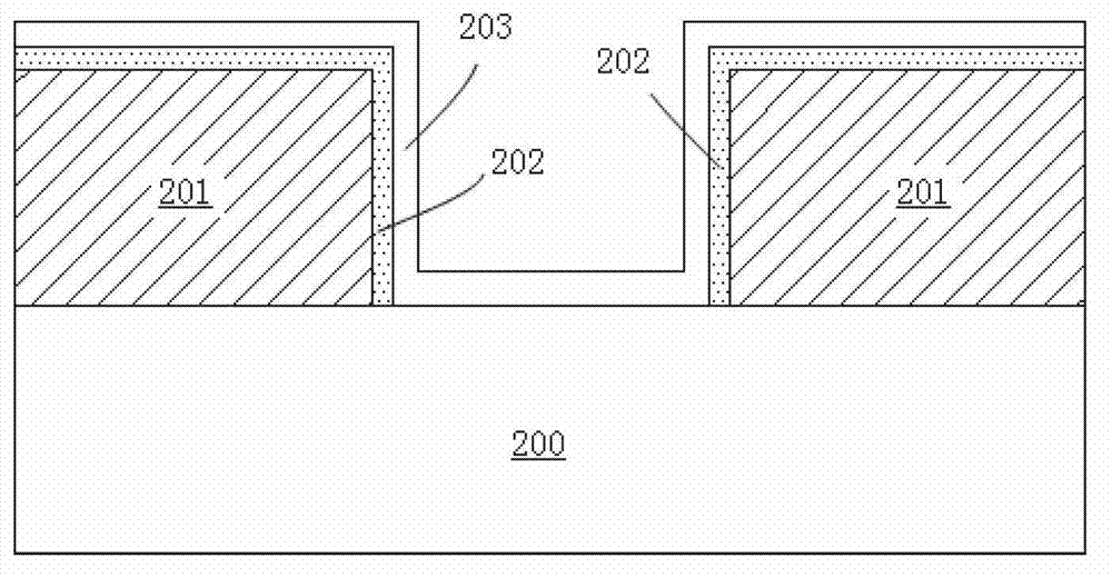
[0029] figure 2 It is a cross-sectional view of an embodiment of the mixed-dielectric anti-copper diffusion barrier layer proposed by the present invention. Such as figure 2 As shown, a low dielectric constant dielectric layer 201 is formed on the semiconductor substrate 200 , and interconnection holes are formed in the low dielectric constant dielectric layer 201 . An oxide layer 202 is formed on the s...


PUM


Abstract

The invention belongs to the field of fabrication and interconnection of integrated circuits, and particularly relates to a mixed-media copper-diffusion-resistant blocking layer for copper interconnection and a manufacturing method of the blocking layer. The mixed-media copper-diffusion-resistant blocking layer has the advantages that the mixed media (oxidation layer / metal) is used as the copper-diffusion-resistant blocking layer, so that (1) the diffusion resistance of metal on copper can be effectively enhanced, the blocking layer is effectively prevented from being oxidized and falling, and the service life of the diffusion blocking layer is prolonged; (2) the effective dielectric constant value of interconnected circuits can be reduced, and further the whole RC delay of the interconnected circuits is reduced; and (3) since the metal and copper have good adhesion and contact, copper can be directly electroplated on the surface of the metal without depositing a layer of copper seed crystal firstly, so that the process is simple and feasible, and is expected to be applied to fabrication of the diffusion blocking layer of copper interconnection in future.

Description

technical field [0001] The invention belongs to the field of integrated circuit manufacturing and interconnection, and in particular relates to a mixed medium (oxidation layer / metal) anti-copper diffusion barrier layer for copper interconnection and a manufacturing method thereof. Background technique [0002] Copper interconnection technology refers to a new semiconductor manufacturing process technology that uses copper metal materials to replace traditional aluminum metal interconnection materials in the manufacture of semiconductor integrated circuit interconnection layers. Traditional copper interconnect structures such as figure 1 As shown, it includes a low dielectric constant dielectric layer 11 formed on a semiconductor substrate 10, an interconnection hole is formed in the low dielectric constant dielectric layer 11, and a bottom wall and a sidewall covering the interconnection hole are formed with An anti-copper diffusion barrier layer 12, a copper metal intercon...

Claims


Application Information

Patent Timeline
Patent Type & Authority Applications(China)
IPC IPC(8): H01L23/532H01L21/768
CPCH01L2924/0002H01L21/486H01L23/481H01L21/76877H01L21/76846H01L21/76831H01L21/76843H01L23/53238H01L23/53295H01L2924/00
Inventor 孙清清房润辰郑珊张卫王鹏飞周鹏
Owner FUDAN UNIV
Why Eureka
Try Eureka