TFT array substrate

a technology of array substrate and thin film transistor, applied in the field of display technology, can solve the problems of displaying effect showing defect, difference in charging rate between sub-pixels, etc., and achieve the effect of preventing incorrect charging, reducing resistance-capacitance delay, and reducing overall resistance of data lines

Active Publication Date: 2016-08-25
TCL CHINA STAR OPTOELECTRONICS TECH CO LTD
View PDF0 Cites 15 Cited by
  • Summary
  • Abstract
  • Description
  • Claims
  • Application Information

AI Technical Summary

Benefits of technology

[0009]An object of the present invention is to provide a thin-film transistor (TFT) array substrate, wherein within a displaying period of a frame of image, the sub-pixels that have inconsistent brightness / darkness are alternate with each other spatially so that a displaying defect of vertical bright / dark lines is improved and since the overall resistance of a data line is reduced, resistance-capacitance delay is reduced so as to prevent incorrect charging at a tail end of a scan line or a data line.
[0024]The efficacy of the present invention is that the present invention provides a TFT array substrate, which changes the way that sub-pixels are arranged so that during a displaying period of a frame of image, the sub-pixels that have inconsistent brightness / darkness become alternate with each other spatially so that a displaying defect of vertical bright / dark lines can be improved and the overall resistance of the data line can be reduced to thereby reduce resistance-capacitance delay and prevent incorrect charging at a tail end of a scan line or a data line.

Problems solved by technology

For example, at a tail end of a data line (or a scan line), the delay in the data line (or the scan line) could cause difference in charging rates between sub-pixels of the odd row and the sub-pixel of the even rows, and consequently, display defects of vertical bright and dark lines may result.
As such, the even-column sub-pixels that are driven first may suffer being insufficiently charged so that the site corresponding to the even-column sub-pixels become insufficiently bright, making the overall displaying effect showing a defect of vertical bright and dark lines.

Method used


Image

  • TFT array substrate
  • TFT array substrate
  • TFT array substrate

Examples


first embodiment

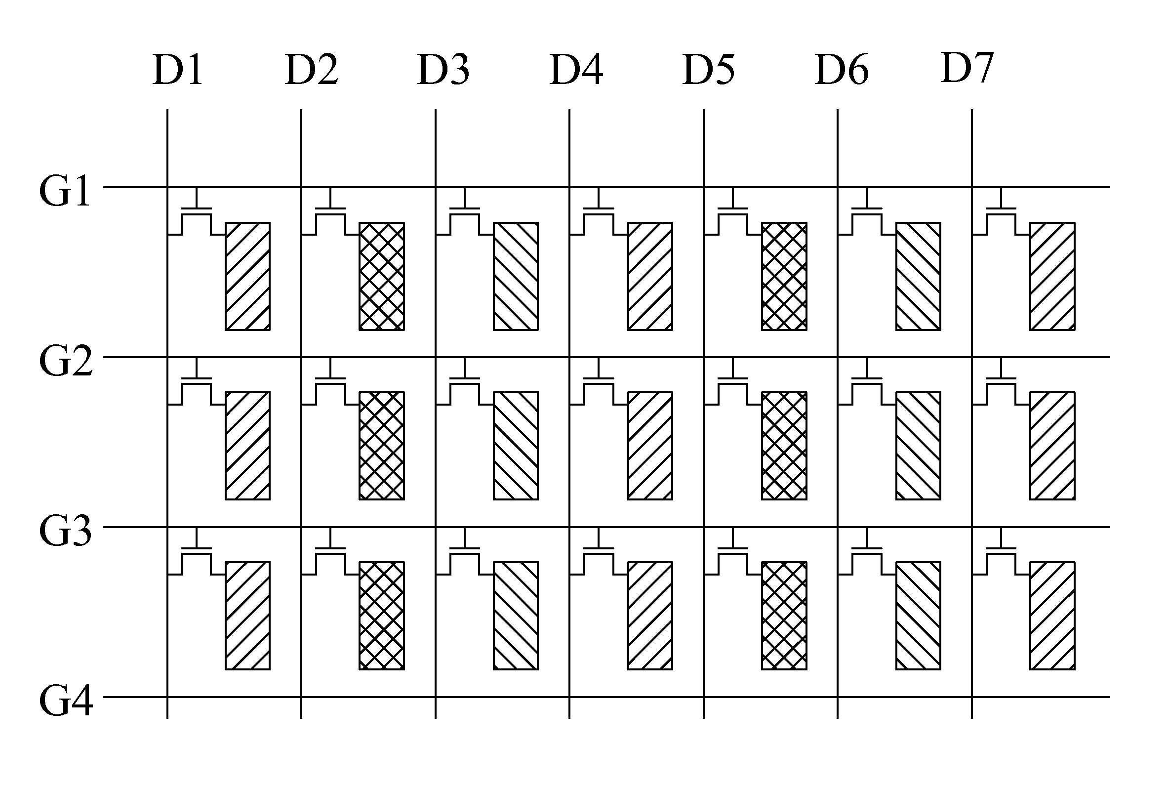
[0036]Referring to FIG. 5, a schematic view is given to illustrate a thin-film transistor (TFT array substrate) according to the present invention. The TFT array substrate comprises: a plurality of data lines, such as D1, D2, D3, D4, a plurality of scan lines, and a plurality of sub-pixels arranged in an array.

[0037]In each row of the sub-pixels, the sub-pixels of odd columns and the sub-pixels of even columns are staggered laterally on a plane.

[0038]Each of the data lines is electrically connected to two sub-pixels of each sub-pixel row that are located on left side and right side of the data line respectively by TFTs and supplies data signals to the two sub-pixels.

[0039]Two scan lines are provided, corresponding to and located at upper and lower sides of each sub-pixel row. The nth scan line G(n) and the (n′)th scan line G(n′) are respectively located on the upper and lower sides of the nth sub-pixel row P(n); the (n+1)th scan line G(n+1) and the (n′+1)th scan line G(n′+1) are res...

second embodiment

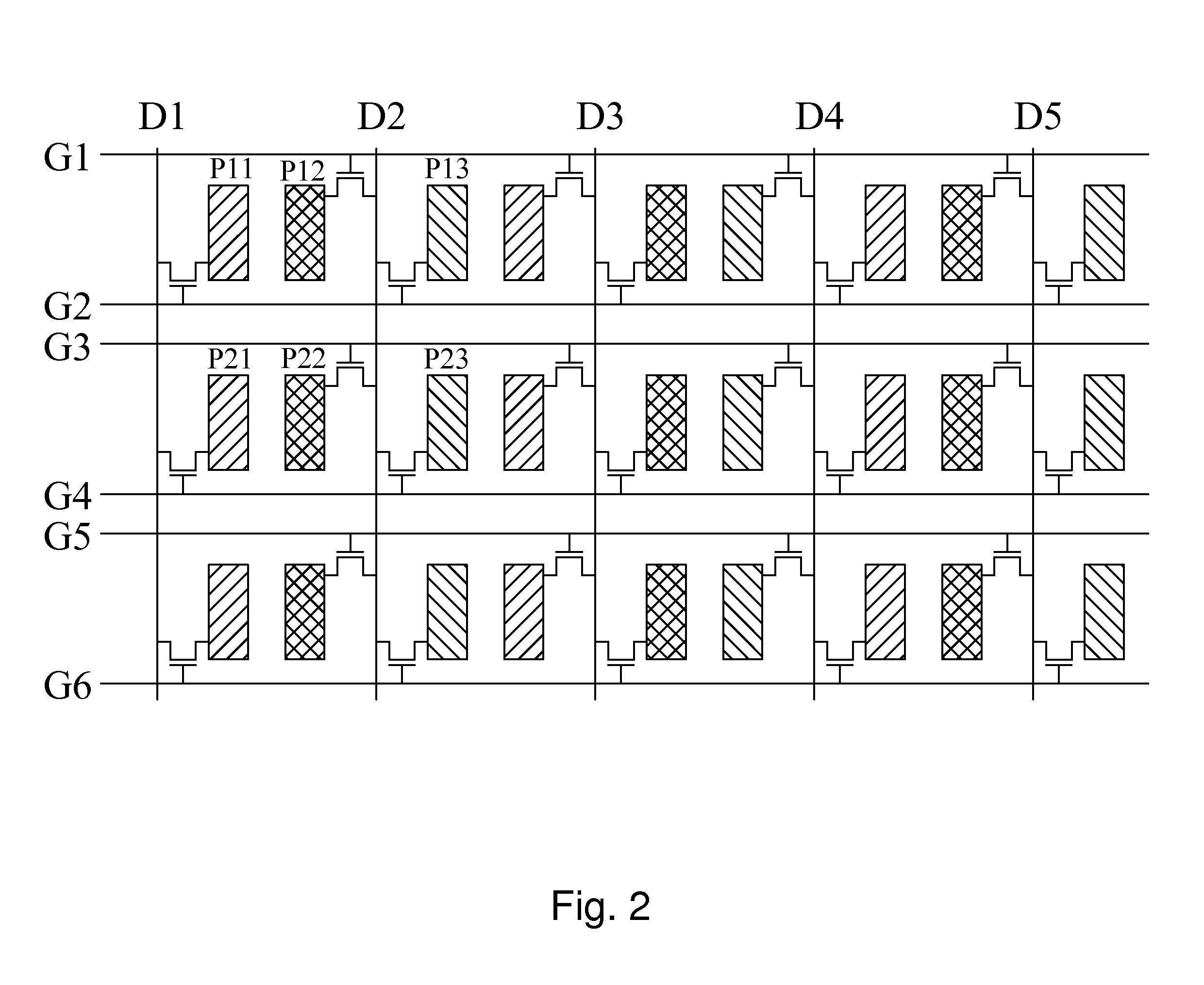
[0043]Referring to FIG. 6, a schematic view is given to illustrate a TFT array substrate according to the present invention. The TFT array substrate comprises: a plurality of data lines, a plurality of scan lines, and a plurality of sub-pixels arranged in an array.

[0044]In each row of the sub-pixels, the sub-pixels of odd columns and the sub-pixels of even columns are staggered laterally on a plane.

[0045]Each of the data lines is electrically connected to two sub-pixels of each sub-pixel row that are located on left side and right side of the data line respectively by TFTs and supplies data signals to the two sub-pixels.

[0046]Two scan lines are provided, corresponding to and located at upper and lower sides of each sub-pixel row. The nth scan line G(n) and the (n′)th scan line G(n′) are respectively located on the upper and lower sides of the nth sub-pixel row P(n); the (n+1)th scan line G(n+1) and the (n′+1)th scan line G(n′+1) are respectively located on the upper and lower sides ...


PUM


Abstract

The present invention provides a thin-film transistor (TFT) array substrate. The TFT array substrate is structured to change the way that sub-pixels are arranged so that during a displaying period of a frame of image, the sub-pixels that have inconsistent brightness / darkness become alternate with each other spatially so that a displaying defect of vertical bright / dark lines can be improved and the overall resistance of the data line can be reduced to thereby reduce resistance-capacitance delay and prevent incorrect charging at a tail end of a scan line or a data line.

Description

BACKGROUND OF THE INVENTION[0001]1. Field of the Invention[0002]The present invention relates to the field of displaying technology, and in particular to a TFT (Thin-Film Transistor) array substrate.[0003]2. The Related Arts[0004]In the field of displaying technology, flat panel displays, such as liquid crystal displays (LCDs) and organic light-emitting diodes (OLEDs) have gradually taken the place of cathode ray tube (CRT) displays for wide applications in liquid crystal televisions, mobile phones, personal digital assistants (PDAs), digital cameras, computer monitors, and notebook computer screens.[0005]A display panel is a major component of the LCDs and OLEDs. Both the LCD display panels and the OLED display panels comprise a thin-film transistor (TFT) array substrate. The TFT array substrate comprises a plurality of red (R), green (G), and blue (B) sub-pixels arranged in an array and a plurality of scan lines and a plurality of data lines. Each of the sub-pixels receives a scan...

Claims


Application Information

Patent Timeline
Patent Type & Authority Applications(United States)
IPC IPC(8): H01L27/12G09G3/3275G09G3/36G09G3/3266
CPCG02F1/13G02F1/1362G09G3/3266G09G3/3275H01L27/124G09G3/3688G09G2300/0809G09G2310/0278G09G3/3677G02F1/136286G09G3/3614G09G2320/0233G09G3/3659G09G2320/0223
Inventor CHEN, CAIQINHSU, JEHAO
Owner TCL CHINA STAR OPTOELECTRONICS TECH CO LTD
Why Eureka
Try Eureka