TFT array substrate
a thin film transistor and array substrate technology, applied in static indicating devices, non-linear optics, instruments, etc., can solve the problems of affecting the overall displaying effect, the difference in charging rate between sub-pixels, etc., to reduce the resistance-capacitance delay, prevent incorrect charging, and reduce the overall resistance of the data line
- Summary
- Abstract
- Description
- Claims
- Application Information
AI Technical Summary
Benefits of technology
Problems solved by technology
Method used
Image
Examples
first embodiment
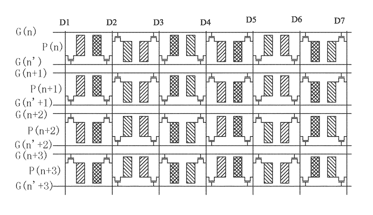
[0037]Referring to FIG. 5, a schematic view is given to illustrate a thin-film transistor (TFT array substrate) according to the present invention. The TFT array substrate comprises: a plurality of data lines, such as D1, D2, D3, D4, D5, D6, D7, a plurality of scan lines, and a plurality of sub-pixels arranged in an array.
[0038]In each row of the sub-pixels, a pair of sub-pixels that are arranged between two adjacent ones of the data lines are in alignment with each other and in each row of the sub-pixels, an odd pair of sub-pixels and an even pair of sub-pixels that are adjacent to each other are staggered laterally on a plane.
[0039]Each of the data lines is electrically connected to two sub-pixels of each sub-pixel row that are located on left side and right side of the data line respectively by TFTs and supplies data signals to the two sub-pixels.
[0040]Two scan lines are provided, corresponding to and located at upper and lower sides of each sub-pixel row. The nth scan line G(n) ...
second embodiment
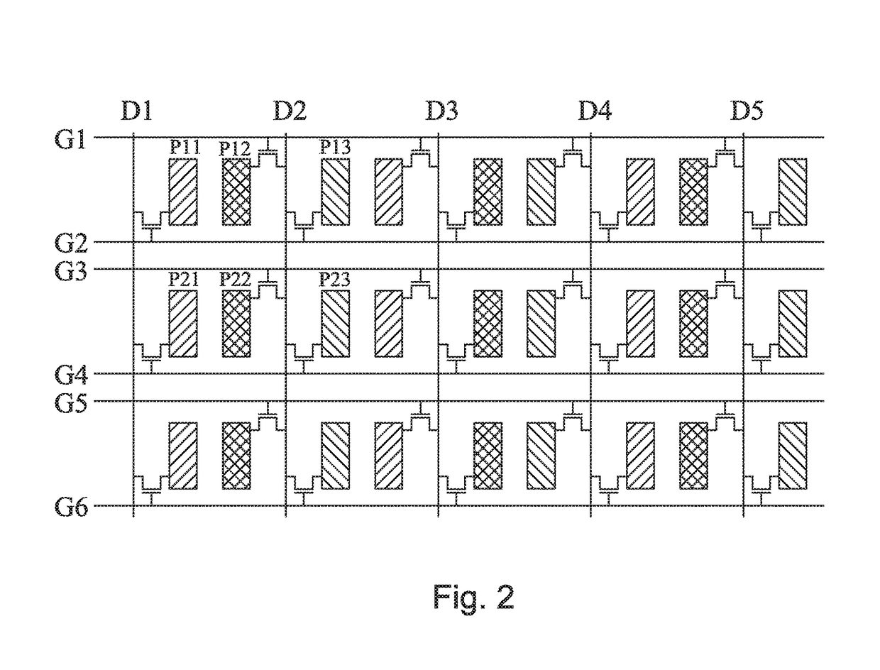
[0044]Referring to FIG. 6, a schematic view is given to illustrate a TFT array substrate according to the present invention. The TFT array substrate comprises:
[0045]a plurality of data lines, a plurality of scan lines, and a plurality of sub-pixels arranged in an array.
[0046]In each row of the sub-pixels, a pair of sub-pixels that are arranged between two adjacent ones of the data lines are in alignment with each other and in each row of the sub-pixels, an odd pair of sub-pixels and an even pair of sub-pixels that are adjacent to each other are staggered laterally on a plane.
[0047]Each of the data lines is electrically connected to two sub-pixels of each sub-pixel row that are located on left side and right side of the data line respectively by TFTs and supplies data signals to the two sub-pixels.
[0048]Two scan lines are provided, corresponding to and located at upper and lower sides of each sub-pixel row. The nth scan line G(n) and the (n′)th scan line G(n′) are respectively locate...
PUM
| Property | Measurement | Unit |
|---|---|---|
| polarity | aaaaa | aaaaa |
| brightness | aaaaa | aaaaa |
| charging time | aaaaa | aaaaa |
Abstract
Description
Claims
Application Information


