Manufacturing method for MOSFET adopting separated trench side gate structure with shield gate

A manufacturing method and shielding gate technology, which is applied in the manufacture of semiconductor/solid-state devices, electrical components, circuits, etc., can solve the problems of large gate-source leakage, reduce gate resistance, and ineffective bonding, so as to eliminate gate-drain capacitance, Effect of reducing gate resistance and reducing parasitic resistance

Active Publication Date: 2016-05-04
SHANGHAI HUAHONG GRACE SEMICON MFG CORP
View PDF5 Cites 14 Cited by
  • Summary
  • Abstract
  • Description
  • Claims
  • Application Information

AI Technical Summary

Problems solved by technology

This method requires a large number of thermal processes to anneal the polysilicon to reduce the gate resistance. In addition, the well region cannot effectively fit the polysilicon gate, resulting in additional gate-to-drain capacitance.
[0013] In addition, in the above existing method, the oxide layer isolated between the other side of the polysilicon gate 106 and the source polysilicon 105, that is, the gate-source isolation oxide layer is formed simultaneously with the gate oxide layer, which makes the gate-source isolation oxide layer and the gate oxide layer layer is as thin as the

Method used


Image

  • Manufacturing method for MOSFET adopting separated trench side gate structure with shield gate
  • Manufacturing method for MOSFET adopting separated trench side gate structure with shield gate
  • Manufacturing method for MOSFET adopting separated trench side gate structure with shield gate

Examples


Embodiment Construction

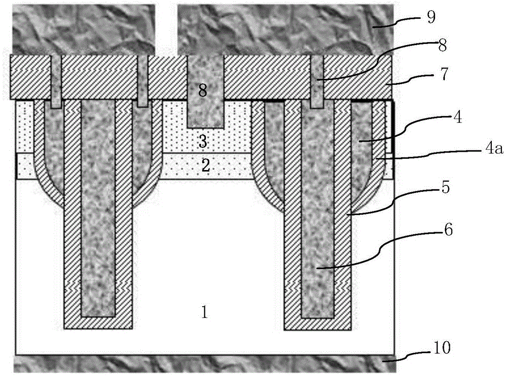
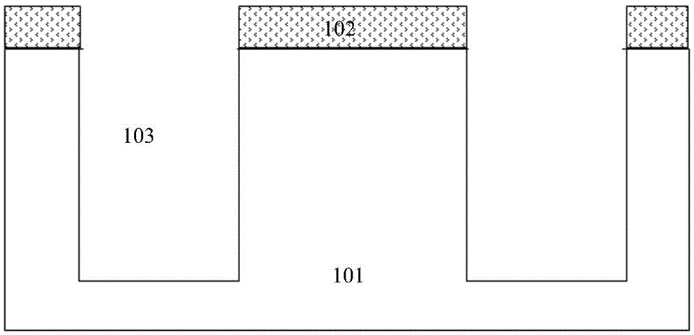
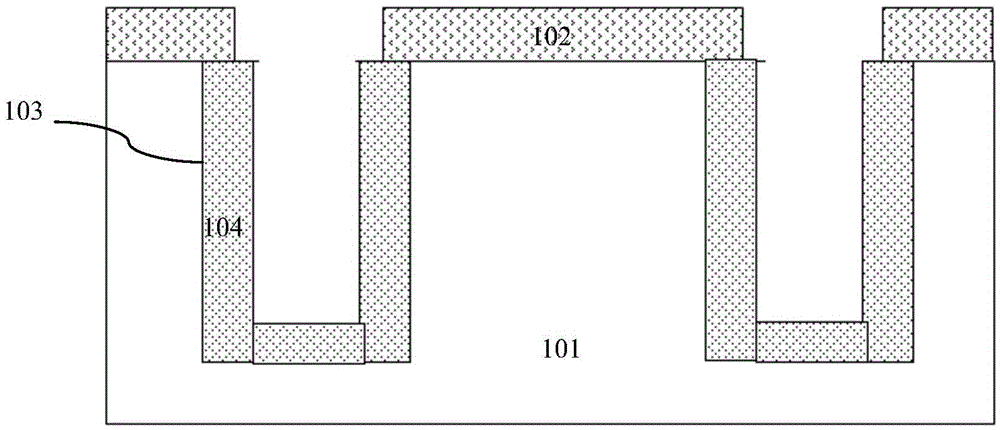
[0045] Such as figure 2 Shown is the flow chart of the method of the embodiment of the present invention; Figure 3A to Figure 3Q Shown is a schematic diagram of the device structure in each step of the method of the embodiment of the present invention. A method for manufacturing a trench-separated side-gate MOSFET with a shield gate in an embodiment of the present invention includes the following steps:

[0046] Step 1, such as Figure 3A As shown, a semiconductor substrate 1 is provided, and ion implantation is performed to form a well region 2 in the semiconductor substrate 1; heavily doped source implantation is performed to form a source region 3 on the surface of the well region 2; 2 and the source region 3 undergo a thermal annealing process. Preferably, the step of forming a shielding oxide layer 201 on the surface of the semiconductor substrate 1 is also included before the ion implantation of the well region 2 and the source region 3, and ions pass through the sh...


PUM


Abstract

The invention discloses a manufacturing method for a MOSFET adopting a separated trench side gate structure with a shield gate. The manufacturing method comprises the steps of performing injection for a well region and a source region in a semiconductor substrate and performing an annealing-boosting process; forming a hard mask layer, and performing a photoetching process to define a gate formation region; performing anisotropic etching for the first time to form a trench; performing anisotropic etching for the second time to increase the width and the depth of the trench; forming a gate dielectric layer and a gate metal layer; performing back etching on the gate metal layer; performing anisotropic etching for the semiconductor substrate at the bottom of the trench; forming oxide layers on the internal surface of the deep trench and the side face of the gate metal layer at the same time; and performing source shield metal layer growth. According to the manufacturing method, the gate resistance can be lowered, the application of the device in a high-frequency circuit is expanded by reducing RC delay, technological steps in a thermal process are reduced, the product manufacturing period is shortened, gate drain capacitance can be lowered, the thickness of the gate source isolating oxide layer can be improved, and the gate source electric leakage can be reduced.

Description

technical field [0001] The invention relates to a method for manufacturing a semiconductor integrated circuit, in particular to a method for manufacturing a trench-separated side-gate MOSFET with a shield gate (ShieldGateTrench, SGT). Background technique [0002] Such as Figure 1A to Figure 1F As shown, it is a schematic diagram of the device structure in each step of the manufacturing method of the existing trench-separated side-gate MOSFET with a shielded gate; this method adopts a bottom-up method to form a trench-separated side-gate structure with a shielded gate, Including the following steps: [0003] Step 1, such as Figure 1A As shown, a semiconductor substrate such as a silicon substrate 101 is provided; a hard mask layer 102 is formed on the surface of the semiconductor substrate 101, and the hard mask layer 102 can be an oxide layer, or an oxide layer plus a nitride layer. Afterwards, the hard mask layer 102 is etched by photolithography to define a gate forma...

Claims


Application Information

Patent Timeline
Patent Type & Authority Applications(China)
IPC IPC(8): H01L21/336H01L29/423
CPCH01L29/42372H01L29/66734H01L29/407H01L29/7813H01L29/41766
Inventor 范让萱缪进征
Owner SHANGHAI HUAHONG GRACE SEMICON MFG CORP
Why Eureka
Try Eureka