SiGe HETEROJUNCTION BIPOLAR TRANSISTOR MULTI-FINGER STRUCTURE

a bipolar transistor and multi-finger technology, applied in the direction of semiconductor devices, basic electric elements, electrical equipment, etc., can solve the problems of still not fully satisfying the rf application requirement, difficult to get f/sub>t above 40 ghz, and expensive to develop advanced cmos technology to get higher f/sub>t. , to achieve the effect of dramatically reducing the effective collector resistance, reducing the distance that the collector current passes, and dramatically reducing the current density

Active Publication Date: 2011-06-23
SHANGHAI HUAHONG GRACE SEMICON MFG CORP
View PDF0 Cites 19 Cited by
  • Summary
  • Abstract
  • Description
  • Claims
  • Application Information

AI Technical Summary

Benefits of technology

[0009]The objective of the present invention is to provide a SiGe HBT multi-finger structure, which can reduce capacitance, decrease collector output resistance, and improve frequency characteristics.
[0014]The benefits of the present invention are: the junction capacitance is much smaller than that of a conventional device as heavily doped ion implantation is only carried out at the bottom of the shallow trench isolations to form the buried layer. By changing the multi-finger structure from C / BE / BE / BE / BE... / C to C / BEBC / BEBC / BEBC / ... / C, the entire multi-finger structure contains more collectors that each emitter can be equipped with a collector, so that the current density can be dramatically reduced for every single collector and the buried layer.
[0015]The distance that the collector current passes is reduced from conventionally passing through the entire multi-finger structure to shorter than the distance of a single cell, as a result, the effective collector resistance can be dramatically decreased, thus improving the cut off frequency characteristics without increasing the total area of the multi-finger structure.

Problems solved by technology

Although higher fT can be achieved by advanced RFCMOS technology, it is still unable to fully satisfy RF application requirement.
For example, it is difficult to get fT above 40 GHz.
It is also very costly to develop advanced CMOS technology to get higher fT.
The devices with compound semiconductor material can get very high fT, but the usage is restricted due to higher material cost, lower wafer size and poisonous nature of most of compound semiconductor material.
But the main disadvantages are: a buried layer of large size is formed through the whole multi-finger device to connect the two collectors at the outmost sides, which leads to large junction capacitance, and impacts the device speed.

Method used


Image

  • SiGe HETEROJUNCTION BIPOLAR TRANSISTOR MULTI-FINGER STRUCTURE
  • SiGe HETEROJUNCTION BIPOLAR TRANSISTOR MULTI-FINGER STRUCTURE
  • SiGe HETEROJUNCTION BIPOLAR TRANSISTOR MULTI-FINGER STRUCTURE

Examples


Embodiment Construction

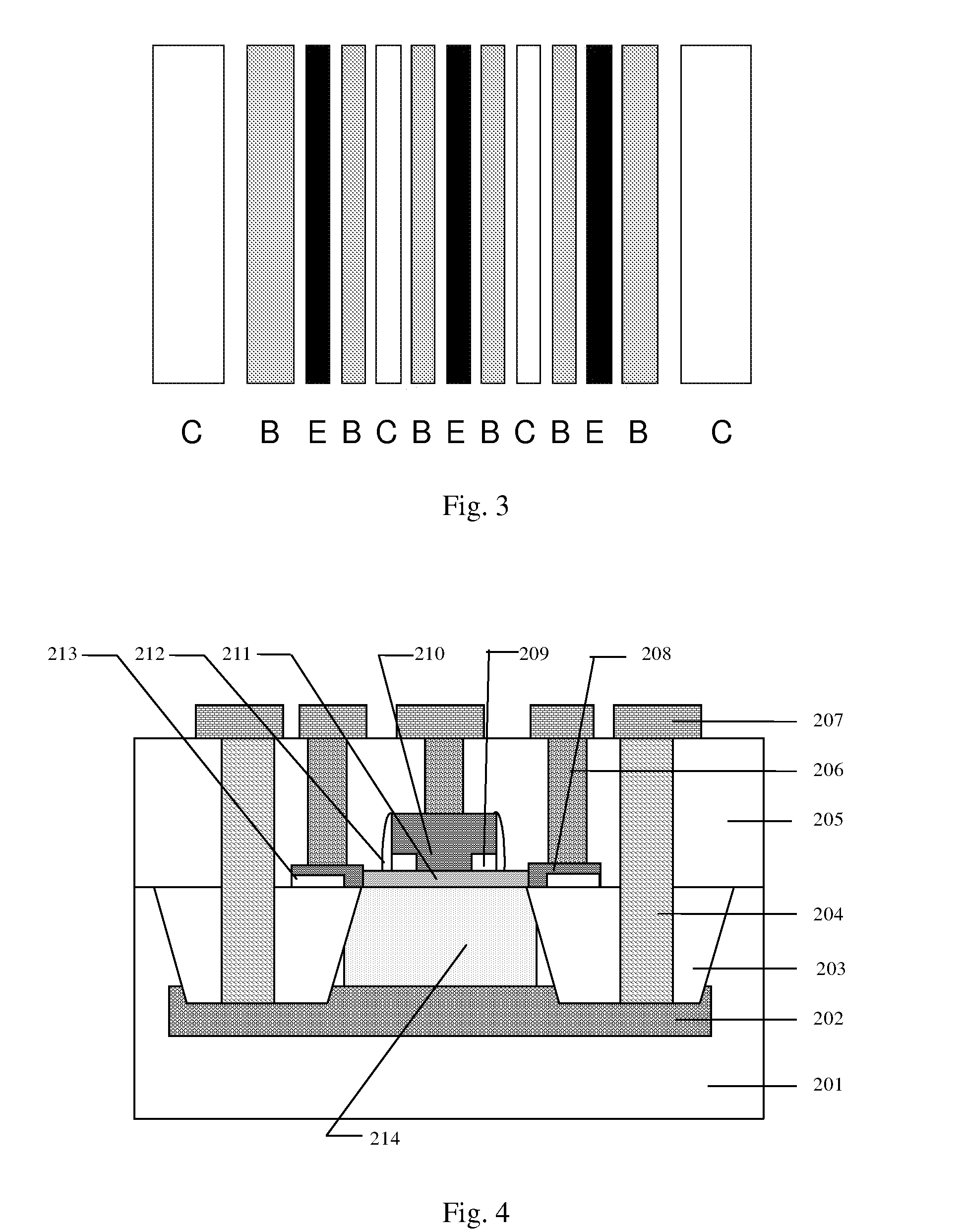
[0021]As illustrated in FIG. 3, the SiGe HBT multi-finger structure of the present invention consists of multiple SiGe HBT single cells. The structure can be denoted by E (emitter), B (base) and C (collector) as C / BEBC / BEBC / BEBC / ... / C, wherein CBEBC represents a single cell of the SiGe HBT, and C is shared by neighboring single cells of the SiGe HBT.

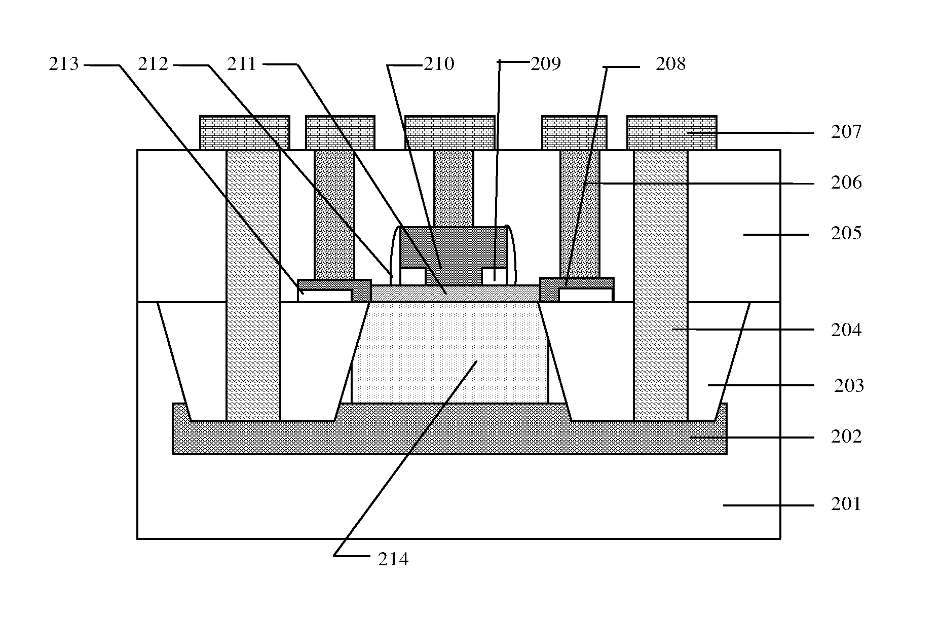
[0022]FIG. 4 illustrates a single cell of the SiGe HBT multi-finger structure of the present invention. The active regions of the SiGe HBT single cell are isolated by field oxide STI (shallow trench isolation). The single cell includes a collector region 214, a base region 211, and an emitter region 210. The collector region 214 is formed by an n type impurity ion implanted layer in the active region. The bottom of the collector region 214 is connected to a buried layer formed by two n type pseudo buried layers 202 in the substrate 201. The two pseudo buried layers 202 are formed by n type impurity ion implantation to the bottom of the s...


PUM


Abstract

The present invention provides a multi-finger structure of a SiGe heterojunction bipolar transistor (HBT). It is consisted of plural SiGe HBT single cells. The multi-finger structure is in a form of C / BEBC / BEBC / ... / C, wherein, C, B, E respectively stands for collector, base and emitter; CBEBC stands for a SiGe HBT single cell. The collector region is consisted of an n type ion implanted layer inside the active region. The bottom of the implanted layer is connected to two n type pseudo buried layers. The two pseudo buried layers are formed through implantation to the bottom of the shallow trenches that surround the collector active region. Two collectors are picked up by deep trench contact through the field oxide above the two pseudo buried layers. The present invention can reduce junction capacitance, decrease collector electrode output resistance, and improve device frequency characteristics.

Description

BACKGROUND OF THE INVENTION[0001]1. Field of the invention[0002]The present invention generally relates to a semiconductor device structure and the manufacturing process thereof, more particularly to the design and fabrication of a high driving current multi finger bipolar transistor device.[0003]2. Description of Related Art[0004]In radio frequency (RF) application, higher device cut off frequency (fT) is needed. Although higher fT can be achieved by advanced RFCMOS technology, it is still unable to fully satisfy RF application requirement. For example, it is difficult to get fT above 40 GHz. It is also very costly to develop advanced CMOS technology to get higher fT. The devices with compound semiconductor material can get very high fT, but the usage is restricted due to higher material cost, lower wafer size and poisonous nature of most of compound semiconductor material.[0005]SiGe HBT is a good choice of high fT devices. Firstly, the emitter injection efficiency and current gain...

Claims


Application Information

Patent Timeline
Patent Type & Authority Applications(United States)
IPC IPC(8): H01L29/737
CPCH01L29/0692H01L29/7378H01L29/0821
Inventor CHIU, TZUYINZHOU, ZHENGLIANGCHEN, XIONGBIN
Owner SHANGHAI HUAHONG GRACE SEMICON MFG CORP
Why Eureka
Try Eureka