Display device and its driving method

a technology of a display device and a driving method, which is applied in the direction of electric digital data processing, instruments, computing, etc., can solve the problems of difficult design of pixel circuits and drive circuits, difficult to make large-area circuits, and difficult to suppress variations in luminance of organic el elements, so as to reduce the scale and area of pixel circuits, reduce the effect of amplitude of data voltage and reduced scal

Active Publication Date: 2010-02-25
SHARP KK
View PDF14 Cites 133 Cited by
  • Summary
  • Abstract
  • Description
  • Claims
  • Application Information

AI Technical Summary

Benefits of technology

[0037]According to the first or eleventh aspect of the present invention, it is possible to read the voltage which depends on the threshold voltage of the drive element from the selected pixel circuit and to apply, to the control terminal of the drive element, the voltage obtained by adding or subtracting the correction voltage (the voltage corresponding to the threshold voltage) to or from the data voltage. Accordingly, it is possible to detect the threshold voltage of the drive element to compensate variations in threshold voltage, and to allow the electro-optical element to emit light at a desired luminance. Moreover, the threshold value correction circuit is provided outside the pixel circuit and the threshold voltage is detected by use of the data line, leading to reduction in scale and area of the pixel circuit. Further, the threshold voltage is detected as a voltage signal, so that a current-voltage conversion element becomes unnecessary unlike a case where an electric current signal is fed back. Therefore, variations in correction effect can be suppressed. Moreover, a desired voltage is applied to the control terminal of the drive element through no coupling capacitance. Therefore, it is possible to efficiently utilize an amplitude of the data voltage and to reduce power consumption.
[0038]According to the second aspect of the present invention, it is possible to reduce the capacitance to be used for threshold value correction, to improve an aperture ratio and a yield, and to reduce power consumption.
[0039]According to the third aspect of the present invention, it is possible to divide the period for selecting the pixel circuit into a period for detecting the threshold voltage and a period for writing the corrected data voltage, and to allow commonality of a feedback line for reading the threshold voltage and a data line for writing the data.
[0040]According to the fourth or fifth aspect of the present invention, it is possible to reduce the number of wiring lines in such a manner that the first to third switching elements share the wiring line to be connected to the control terminals thereof. Thus, it is possible to make an aperture ratio of a pixel higher.
[0041]According to the sixth aspect of the present invention, the variations in threshold voltage can be compensated in the drive element of the P-channel type when the voltage obtained by subtraction of the absolute value of the threshold voltage is applied to the control terminal. Therefore, it is possible to compensate the variations in threshold voltage of the drive element by use of the voltage outputted from the selected pixel circuit.
[0042]According to the seventh aspect of the present invention, the variations in threshold voltage can be compensated in the drive element of the N-channel type when the voltage obtained by addition of the absolute value of the threshold voltage is applied to the control terminal. Therefore, it is possible to compensate the variations in threshold voltage of the drive element by use of the voltage outputted from the selected pixel circuit.

Problems solved by technology

Consequently, it becomes very difficult to suppress the variations in luminance of the organic EL element if a driving scheme of a voltage control type is adopted for the organic EL display.
However, the electric current program scheme has the following two problems.
First, it is difficult to design a pixel circuit and a drive circuit since an electric current to be used herein is considerably small in amount.
Second, it is difficult to make a large-area circuit since an influence of a parasitic capacity is exerted readily when an electric current signal is set.

Method used


Image

  • Display device and its driving method
  • Display device and its driving method
  • Display device and its driving method

Examples


first embodiment

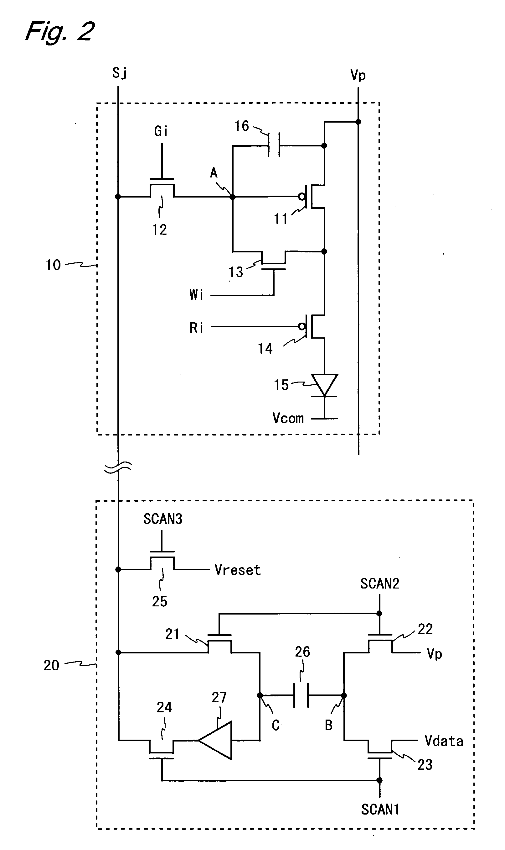
[0088]FIG. 2 is a circuit diagram showing the pixel circuit and the threshold value correction circuit each included in the display device according to the first embodiment of the present invention. The pixel circuit 10 and the threshold value correction circuit 20 in FIG. 2 correspond to the pixel circuit Aij and the threshold value correction circuit 9 in FIG. 1. As shown in FIG. 2, the pixel circuit 10 includes a driving TFT 11, switching TFTs 12 to 14, an organic EL element 15 and a capacitor 16. The driving TFT 11 is of an enhancement P-channel type, each of the switching TFTs 12 and 13 is of an N-channel type, and the switching TFT 14 is of a P-channel type.

[0089]The pixel circuit 10 is connected to the power supply wiring line Vp, the common cathode Vcom, the scanning line Gi, the control line Wi, the control line Ri and the data line Sj. Hereinafter, a potential at the power supply wiring line Vp is represented by VDD and a potential at the common cathode Vcom is represented...

second embodiment

[0132]FIG. 7 is a circuit diagram showing a pixel circuit and a threshold value correction circuit each included in the display device according to the second embodiment of the present invention. The pixel circuit 40 and the threshold value correction circuit 50 in FIG. 7 correspond to the pixel circuit Aij and the threshold value correction circuit 9 in FIG. 1. As shown in FIG. 7, the pixel circuit 40 includes a driving TFT 41, switching TFTs 42 to 44, an organic EL element 45 and a capacitor 46. The driving TFT 41 is of an enhancement N-channel type, and each of the switching TFTs 42 to 44 is of an N-channel type.

[0133]In the pixel circuit 40, the organic EL element 45, the switching TFT 44 and the driving TFT 41 are provided in series between a power supply wiring line Vp and a common cathode Vcom sequentially from a side of the power supply wiring line Vp. The switching TFT 42 is provided between a gate terminal of the driving TFT 41 and a data line Sj. The switching TFT 43 is p...

third embodiment

[0137]In each of the display devices according to the first and second embodiments, the analog buffer 27 is provided for each data line Sj. In a 2-inch QVGA full-color panel (including RGB sub pixels), however, a pitch between the sub pixels is about 42 μm. The capacitor 26 that holds the correction voltage Vx which depends on the threshold voltage of the driving TFT can be arranged at this pitch, but the high-performance analog buffer 27 can not be arranged at this pitch in some instances. In the third embodiment, therefore, description will be given of the display device in which the number of analog buffers 27 is reduced.

[0138]FIG. 9 is a circuit diagram showing a threshold value correction circuit included in the display device according to the third embodiment of the present invention. The threshold value correction circuits 60r, 60g and 60b in FIG. 9 correspond to the threshold value correction circuit 9 in FIG. 1. Moreover, data lines Sj_R, Sj_G and Sj_B in FIG. 9 correspond ...


PUM


Abstract

In a pixel circuit 10, TFTs 12 and 13 are turned on while a TFT 14 is turned off, and a voltage (VDD+Vx) which depends on a threshold voltage Vth of a driving TFT 11 is read onto a data line Sj. Moreover, switches 21 and 22 in a source driver circuit are turned on, and a voltage Vx is held at a capacitor 26. Next, the TFT 13 is turned off, states of switches 21 to 24 are switched, and a voltage (Vdata+Vx) is applied to the data line Sj. Further, the TFT 12 is turned off while the TFT 14 is turned on. An amount of an electric current flowing through an organic EL element 15 after the turn-on of the TFT 14 is determined from the voltage (Vdata+Vx) of a gate terminal of the driving TFT 11. Thus, it is possible to efficiently utilize an amplitude of a data voltage and compensate variations in threshold voltage of the driving TFT 11 with high accuracy, without increasing a scale of the pixel circuit 10.

Description

TECHNICAL FIELD[0001]The present invention relates to display devices, more particularly, to display devices using an electric current driving element such as an organic EL display or an FED, and a method for driving the same.BACKGROUND ART[0002]Recently, there has been increased demand for thin and lightweight display devices achieving high-speed response. Therefore, there has been actively conducted research and development on organic EL (Electro Luminescence) displays and FEDs (Field Emission Displays).[0003]An organic EL element included in an organic EL display emits light at higher luminance as a voltage to be applied thereto is high and an electric current flowing therethrough is large in amount. In the organic EL element, however, a relation between the luminance and the voltage varies readily due to influences such as a driving time and an ambient temperature. Consequently, it becomes very difficult to suppress the variations in luminance of the organic EL element if a driv...

Claims


Application Information

Patent Timeline
Patent Type & Authority Applications(United States)
IPC IPC(8): G09G5/00G09G3/30
CPCG09G3/3233G09G3/3291G09G2320/0295G09G2300/0852G09G2320/0233G09G2300/0819
Inventor KISHI, NORITAKA
Owner SHARP KK
Why Eureka
Try Eureka