Semiconductor device and control method thereof

a technology of semiconductor devices and circuits, applied in the field of semiconductor devices, can solve the problems of reducing the output voltage of the drain pump, and unable to program multiple bits at the same time, so as to achieve the effect of not having to increase the number of the program voltage generation circuits and not enlarging the circuitry scal

Active Publication Date: 2007-06-05
MONTEREY RES LLC
View PDF8 Cites 38 Cited by
  • Summary
  • Abstract
  • Description
  • Claims
  • Application Information

AI Technical Summary

Benefits of technology

[0009]According to an aspect of the present invention, preferably, there is provided a semiconductor device including a program voltage supply circuit that supplies a drain of a memory cell with a program voltage, and a voltage generating circuit that generates a voltage supplied to a gate of the memory cell by using a clock signal based on the program voltage supplied by the program voltage supply circuit. According to the present invention, the gate voltage can be controlled and multiple bits can be programmed simultaneously so as not to exceed the current supply capacity of the program voltage generating circuit, by using the clock signal determined on the basis of the program voltage supplied by the program voltage supply circuit. It is therefore possible to make the best use of the ability of the program voltage generating circuit at the time of programming. Furthermore, the number of the program voltage generating circuits does not have to be increased and the circuitry scale is not enlarged.
[0017]According to another aspect of the present invention, preferably, there is provided a method of controlling a semiconductor device including the steps of supplying a program voltage to a drain of a memory cell, and generating a voltage supplied to a gate of the memory cell by using a clock signal determined based on the program voltage. According to the present invention, the gate voltage can be controlled and multiple bits can be programmed simultaneously so as not to exceed the current supply capacity of the program voltage generating circuit, by using the clock signal determined on the basis of the program voltage supplied by the program voltage supply circuit. It is therefore possible to make the best use of the ability of the program voltage generating circuit at the time of programming. Furthermore, the number of the program voltage generating circuits does not have to be increased and the circuitry scale is not enlarged.

Problems solved by technology

There arises the problem in that the output voltage of the drain pump is decreased and the multiple bits cannot be programmed simultaneously.
In addition, the current supply capacity can be enhanced by increasing the number of the program voltage generating circuits 1, yet this causes another problem of enlarging the circuitry scale.
Further, there is further another problem in that the technique described in Document 1 cannot control the gate voltage correctly.

Method used


Image

  • Semiconductor device and control method thereof
  • Semiconductor device and control method thereof
  • Semiconductor device and control method thereof

Examples


first embodiment

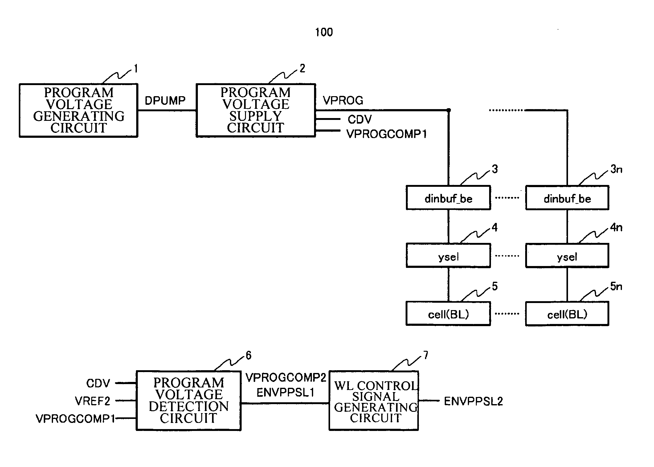
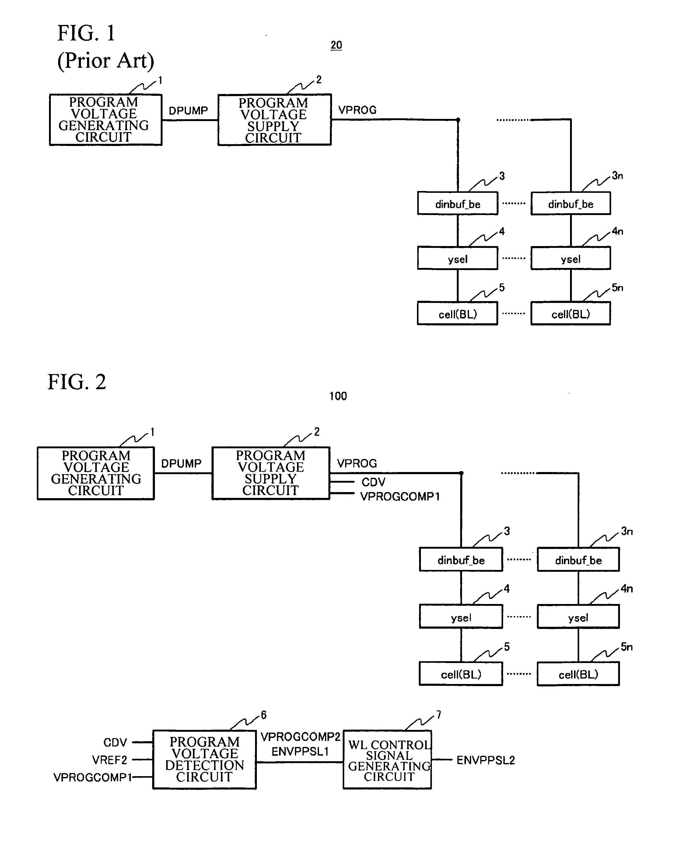
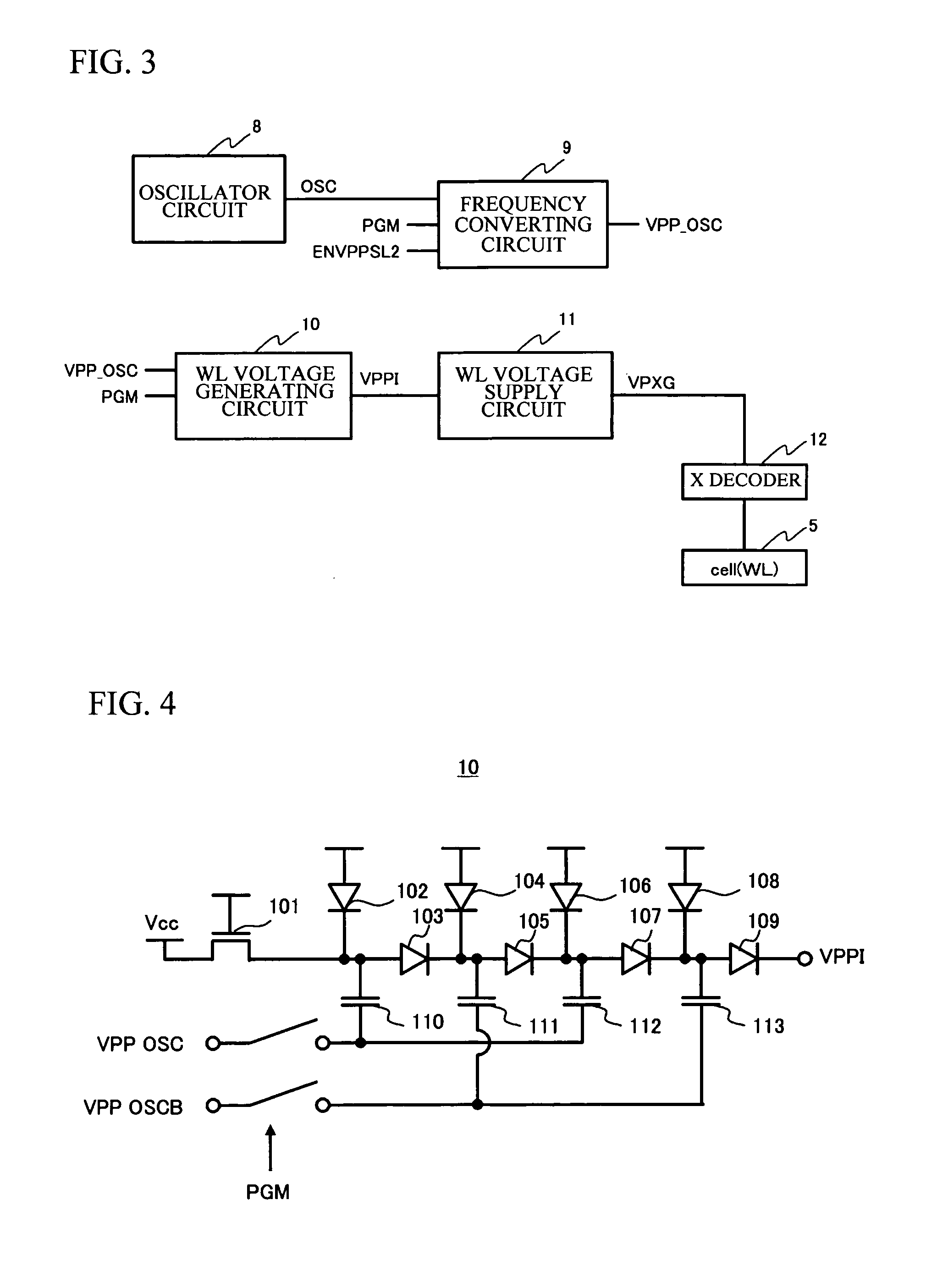
[0036]FIG. 2 is a view partially showing a circuit configuration of the non-volatile semiconductor memory device in accordance with the first embodiment of the present invention. As shown in FIG. 2 and FIG. 3, the non-volatile semiconductor memory device 10 includes a program voltage generating circuit 1, a program voltage supply circuit 2, a data in buffer circuit 3, a Y decoder (ysel) 4, a memory cell 5, a program voltage detection circuit 6, a WL voltage control signal generating circuit 7, an oscillator circuit 8, a frequency converting circuit 9, a WL voltage generating circuit 10, a WL voltage supply circuit 11, and an X decoder 12.

[0037]In the memory cell 5, for example, there are provided an N-type source region and a drain region on a surface of a p-type substrate, and there are also provided a floating gate and control gate on a channel region between the above-mentioned regions. The control gate is connected to the word line WL, the drain region is connected to the bit li...

second embodiment

[0062]Next, a description will be given of a second embodiment. FIG. 11A is a view partially showing a circuit configuration of the non-volatile semiconductor memory device in accordance with the second embodiment. FIG. 12 is a view partially showing a circuit configuration of the non-volatile semiconductor memory device in accordance with the second embodiment. As shown in FIGS. 11A through 11C and FIG. 12, a non-volatile semiconductor memory device 200 includes the program voltage generating circuit 1, the program voltage supply circuit 2, the data in buffer circuit 3, the Y decoder (ysel) 4, the memory cell 5, a WL voltage control signal generating circuit 207, the oscillator circuit 8, the frequency converting circuit 9, the WL voltage generating circuit 10, the WL voltage supply circuit 11, the X decoder 12, and a current detection circuit 213. The gate of the memory cell 5 is controlled by the voltage applied to the word line WL. Pass transistors 41 and 42 are provided for sel...


PUM


Abstract

A semiconductor device including a program voltage supply circuit that supplies a drain of a memory cell with a program voltage, a detection circuit that refers to an output voltage of the program voltage supply circuit and detects a decrease of the program voltage supplied thereby, a frequency converting circuit that generates the clock signal by converting a frequency of a clock signal generated by an oscillator circuit into a lower frequency when the program voltage supplied by the program voltage supply circuit becomes equal to or lower than a given voltage, and a voltage generating circuit that generates a voltage supplied to a gate of the memory cell by using a clock signal, the frequency of which is converted by the frequency converting circuit. It is therefore possible to make the best use of the ability of the program voltage generating circuit in programming.

Description

CROSS REFERENCE TO RELATED APPLICATIONS[0001]This is a continuation of International Application No. PCT / JP2004 / 017806, filed Nov. 30, 2004.BACKGROUND OF THE INVENTION[0002]1. Field of the Invention[0003]This invention relates to a semiconductor device and a control method thereof.[0004]2. Description of the Related Art[0005]FIG. 1 is a view showing a circuit configuration of a conventional non-volatile semiconductor memory device at the time of programming. As shown in FIG. 1, a non-volatile semiconductor memory device 20 includes a program voltage generating circuit 1, a program voltage supply circuit 2, a data in buffer circuit (dinbuf_be) 3, a Y decoder (ysel) 4, and a memory cell 5. The memory cell 5 is a flash memory having a floating gate or a nitride film, serving as a charge accumulation layer. A high voltage is applied to a drain terminal of the memory cell 5 to inject hot carriers into the charge accumulation layer at the time of programming. A high program voltage VPROG ...

Claims


Application Information

Patent Timeline
Patent Type & Authority Patents(United States)
IPC IPC(8): G11C11/34
CPCG11C16/12G11C2216/14
Inventor KOMORI, HIDEKIKAWAMURA, SHOUICHITAYA, MASANORI
Owner MONTEREY RES LLC
Why Eureka
Try Eureka