Hexagonal architecture

a hexagonal structure and hexagonal technology, applied in the field of hexagonal architecture, can solve the problems of increasing the percentage of path delay, affecting the speed of interconnect communication, and affecting the speed of data communication, so as to reduce the total length of the interconnect congestion, reduce parasitic capacitance and other undesirable effects

Inactive Publication Date: 2002-06-18
BELL SEMICON LLC
View PDF13 Cites 244 Cited by
  • Summary
  • Abstract
  • Description
  • Claims
  • Application Information

AI Technical Summary

Benefits of technology

In accordance with one aspect of the present invention, three layers of metal provide electrical conductors for interconnection which extend in three directions that are angularly displaced from each other by 60 degrees, which is sometimes referred to as a tri-directional or hexagonal routing system. This is the preferred embodiment of the polydirectional non-orthogonal three layer metal routing invention. On average, the three direction routing system according to one aspect of the present invention using three metal layers for interconnect will result in a total interconnect wire length that is shorter than the total interconnect wire length required using a conventional two metal layer rectangular routing system. This tri-directional routing can be used in connection with conventional rectangular cells, or it may be advantageously used in conjunction with triangular, hexagonal, diamond, parallelogram shaped cells, as well as any other arbitrary shaped cell.
The three routing directions provided by the present invention substantially reduce the total wirelength interconnect congestion of an integrated circuit. The routing directions include, relative to a first direction, two diagonal directions that provide shorter interconnect paths than conventional rectilinear routing.
In addition, the number of conductors that extend parallel to each other is smaller, and the angles between conductors in different layers are larger than in the prior art, thereby reducing parasitic capacitance and other undesirable effects that result from conventional rectilinear routing.
One embodiment includes a microelectronic integrated circuit that may advantageously utilize the three direction routing arrangement described herein. A triangular device design includes a semiconductor substrate, and a plurality of microelectronic devices that are formed on the substrate in a closely packed triangular arrangement that maximizes the space utilization of the circuit.
Cells can have serrated edges defined by edges of hexagons such that adjacent cells fit together exactly, providing a closely packed arrangement of cells on the substrate with effective utilization of space. Cells can be defined by clusters of two or more hexagons, enabling a variety of cell shapes to be accommodated. Sets of cells having the same functionality and different shapes may be provided.

Problems solved by technology

In the past, the time required for data communication was typically insignificant compared to the time required for computation, and could be neglected.
Now, the interconnection delays are on the order of gate delays and as a result, have become significant and can no longer be ignored.
Interconnect delays are an increasing percentage of path delay.
When two wires in the same metal layer run parallel to each other, parasitic capacitances may be significant and "crosstalk" may occur between signals on those wires.
This has resulted in unsatisfactory capacitance and "crosstalk" in many instances.
Significant performance degradation may result.
In the past, efforts to increase the number of metal layers in an attempt to approach a zero-routing footprint chip have resulted in offsetting performance degradation due to unsatisfactory capacitance and "crosstalk" from parallel wires located in different metal layers.
It is an extremely tedious and an error-prone process because of the tight tolerance requirements, the complexity of the design rules, and the minuteness of the individual components.
Achievement of this goal is restricted using conventional rectilinear routing because diagonal connections are not possible.
Another drawback of conventional rectilinear interconnect routing is its sensitivity to parasitic capacitance.
Since many conductors run in the same direction in parallel with each other, adjacent conductors form parasitic capacitances that can create signal crosstalk and other undesirable effects.
Conventional memory arrays such as DRAMs and SRAMs have been density limited by the metal pitch, which has become a limiting feature inhibiting further shrinkage of the size of the layout.
Wiring congestion, crosstalk, and parasitic capacitance are problems limiting the performance and size of conventional memory arrays.
In the case of a DRAM cell, in particular, the line capacitance can be a problem when it becomes large relative to the storage capacitance of the cell storage devices.
A DRAM memory circuit can only tolerate a certain ratio of line capacitance to storage capacitance.
Conventional designs are limited in the available options to deal with this problem.
However, increasing the cell size tends to increase the size of the layout on a die, and limits the amount of circuitry that can be laid out on a given size die, and may inflict performance penalties.
Large amounts of storage capacitance may slow the speed of a memory array.
This slows the operation of the memory circuit.
The speed of microprocessors and other circuits has become so fast that memory accesses can be a significant limitation upon the performance of a system where access speeds measured in nanoseconds are considered to be slow.
Thus, increased capacitance can be a problem with high performance memory circuits.
Achievement of this goal is restricted using conventional rectilinear routing because diagonal connections are not possible.
Another drawback of conventional rectilinear interconnect routing is its sensitivity to parasitic capacitance.
Since many conductors run in the same direction in parallel with each other, adjacent conductors form parasitic capacitances that can create signal crosstalk and other undesirable effect.
Significantly, that patent does not even recognize the problem of minimizing interconnection wire lengths and interlayer capacitance or "crosstalk."
This patent does not teach or suggest providing three metal layers in a hexagonal architecture preferably employing over-the-cell routing, and does not recognize the problem of minimizing interconnection wire lengths and interlayer capacitance or "crosstalk."
U.S. Pat. No. 5,130,767 does not teach or suggest providing three metal layers in a hexagonal architecture, and does not recognize the problem of minimizing interconnection wire lengths and interlayer "crosstalk."
While in the past satisfactory results were obtained using rectangular architectures employing two layers of metal, those old techniques will not suffice for many new designs incorporating millions of transistors.

Method used


Image

  • Hexagonal architecture
  • Hexagonal architecture
  • Hexagonal architecture

Examples


Embodiment Construction

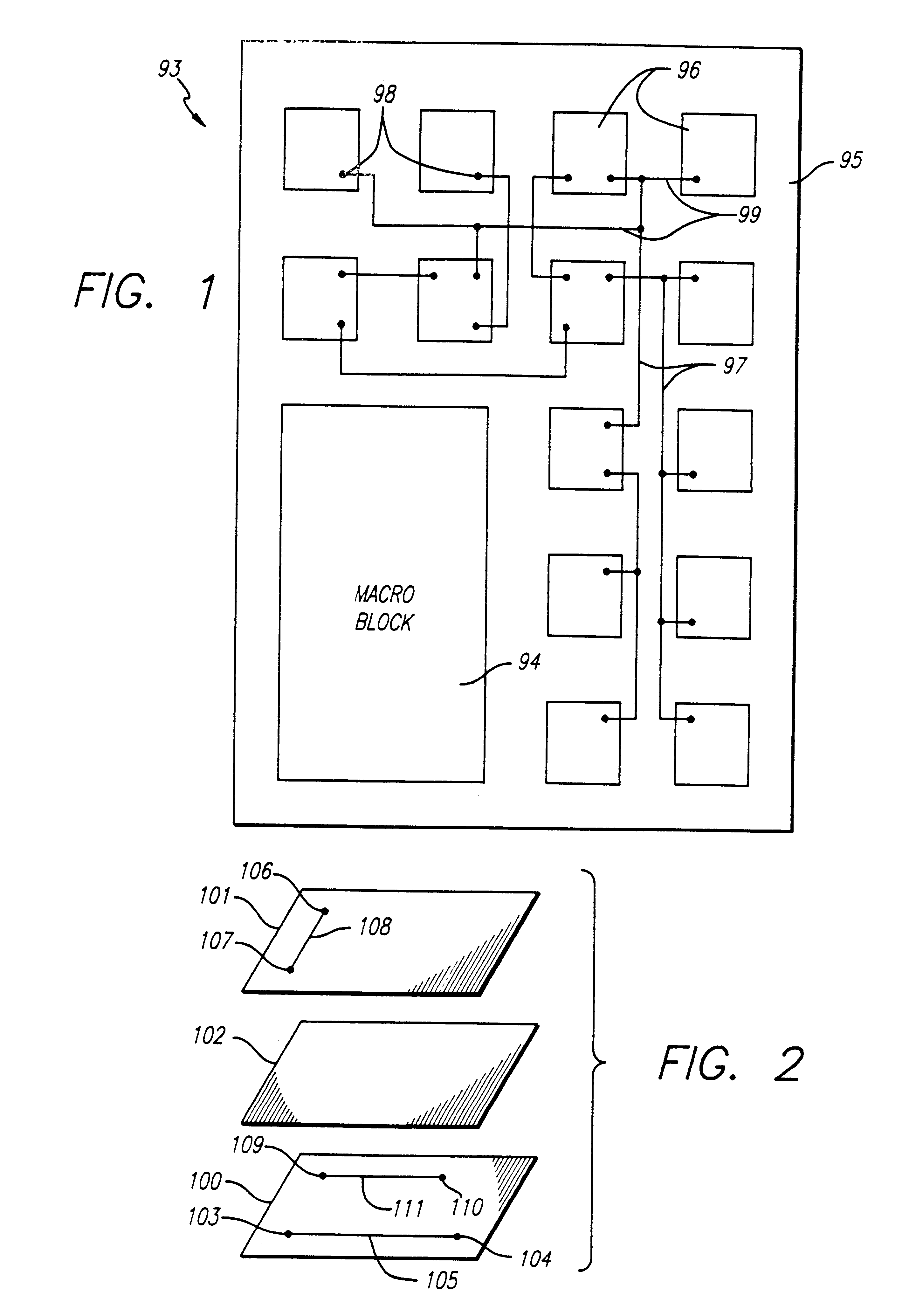
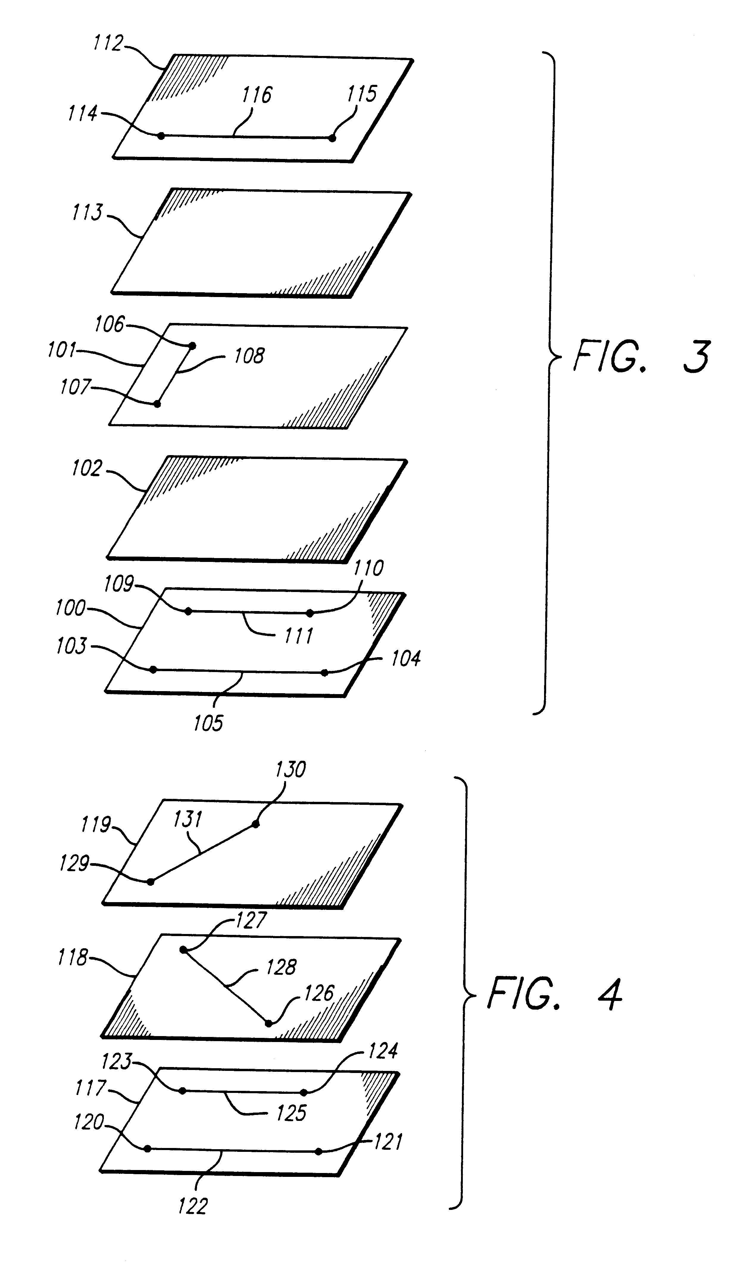
In FIG. 2, two conventional layers of metal are shown schematically. This is an exploded diagram separating the individual layers for clarity. A first metal (M1) layer 100 is shown separated from a second metal (M2) layer 101 by a dielectric layer 102. A conventional rectangular routing arrangement is illustrated. The first metal layer 100 provides for electrical connections in a direction that is angularly displaced 90 degrees from electrical connections provided by the second metal layer 101. For example, in the M1 layer 100, a point 103 is connected to a point 104 by a metal wire 105. In the M2 layer 101, a point 106 is connected to a point 107 by a metal wire 108. The wire 105 is angularly displaced 90 degrees from the wire 108; in other words, the wire 105 in the M1 layer 100 is perpendicular to wire 108 in the M2 layer 101. Wires in the same layer will be parallel to each other. For example, point 109 in the M1 metal layer 100 is connected to point 110 by a wire 111. The wire ...


PUM


Abstract

Several inventions are disclosed. A cell architecture using hexagonal shaped cells is disclosed. The architecture is not limited to hexagonal shaped cells. Cells may be defined by clusters of two or more hexagons, by triangles, by parallelograms, and by other polygons enabling a variety of cell shapes to be accommodated. Polydirectional non-orthogonal three layer metal routing is disclosed. The architecture may be combined with the tri-directional routing for a particularly advantageous design. In the tri-directional routing arraingement, electrical conductors for interconnecting terminals of microelectronic cells of an integrated circuit preferrably extend in three directions that are angularly displaced from each other by 60°. The conductors that extend in the three directions are preferrably formed in three different layers. A method of minimizing wire length in a semiconductor device is disclosed. A method of minimizing intermetal capacitance in a semiconductor device is disclosed. A novel device called a "tri-ister" is disclosed. Triangular devices are disclosed, including triangular NAND gates, triangular AND gates, and triangular OR gates. A triangular op amp and triode are disclosed. A triangular sense amplifier is disclosed. A DRAM memory array and an SRAM memory array, based upon triangular or parallelogram shaped cells, are disclosed, including a method of interconnecting such arrays. A programmable variable drive transistor is disclosed. CAD algorithms and methods are disclosed for designing and making semiconductor devices, which are particularly applicable to the disclosed architecture and tri-directional three metal layer routing.

Description

This specification discloses a plurality of inventions relating generally to the art of microelectronic integrated circuits and electronic systems incorporating such circuits, and the disclosed subject matter may be specifically applied to microelectronic semiconductor integrated circuit structures and methods of designing and manufacturing semiconductor devices.BACKGROUND OF THE DISCLOSUREThe fabrication of semiconductor devices has progressed significantly over the last four decades. Semiconductor chips incorporating over a million transistors are possible. However, the development of technologies such as interactive high-definition television, personal global communications systems, virtual reality applications, real-life graphics animation, and other scientific and industrial applications, will demand higher speed, more functionality, and further advances in very large scale integration technology. The demand for more functionality will require an increase in the number of trans...

Claims


Application Information

Patent Timeline
Patent Type & Authority Patents(United States)
IPC IPC(8): G11C5/02G06F17/50G11C5/06H01L23/522H01L23/52H01L23/528H01L27/11H01L27/108H01L27/085H01L27/02H01L27/118H01L27/092H03K19/0944H03K19/0948H01L29/06
CPCG06F17/5072G06F17/5077G11C5/025G11C5/063H01L23/5222H01L23/528H01L27/0207H01L27/0922H01L27/108H01L27/11H01L27/1104H01L27/11807H03K19/09441H03K19/0948H01L2924/0002H01L29/0657H01L2924/00G06F30/394G06F30/392H10B12/00H10B10/00H10B10/12
Inventor ROSTOKER, MICHAEL D.KOFORD, JAMES S.SCEPANOVIC, RANKOJONES, EDWIN R.PADMANAHBEN, GOBI R.KAPOOR, ASHOK K.KUDRYAVTSEV, VALERIY B.ANDREEV, ALEXANDER E.ALESHIN, STANISLAV V.PODKOLZIN, ALEXANDER S.
Owner BELL SEMICON LLC
Why Eureka
Try Eureka