
Surface Acoustic Wave Device and Communication Device

a surface acoustic wave and waveguide technology, applied in the direction of impedence networks, electrical devices, piezoelectric/electrostrictive/magnetostrictive devices, etc., can solve the problems of unbalanced input, unbalanced output, and difficulty in sufficiently obtaining the gain of an antenna, so as to improve the sharpness of the vicinity of the outside of the lower frequency side of the pass band, improve the insertion loss in the pass band, and enhance the frequency characteristi

Active Publication Date: 2010-10-14
KYOCERA CORP
View PDF12 Cites 19 Cited by
  • Summary
  • Abstract
  • Description
  • Claims
  • Application Information

AI Technical Summary

Benefits of technology

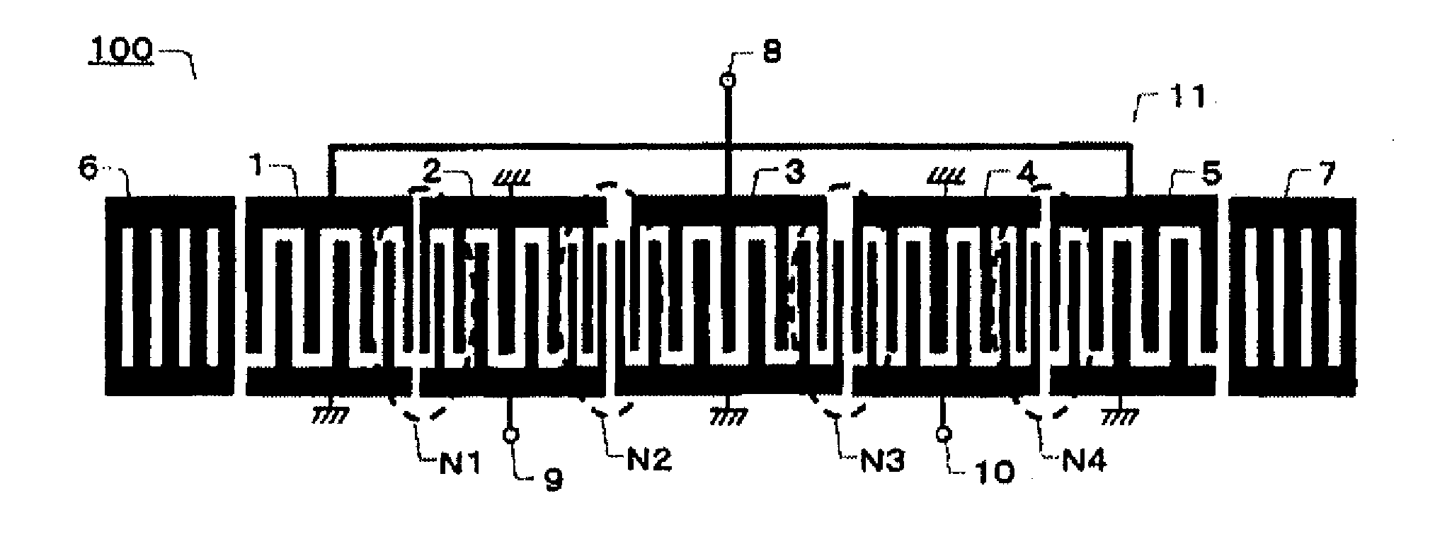
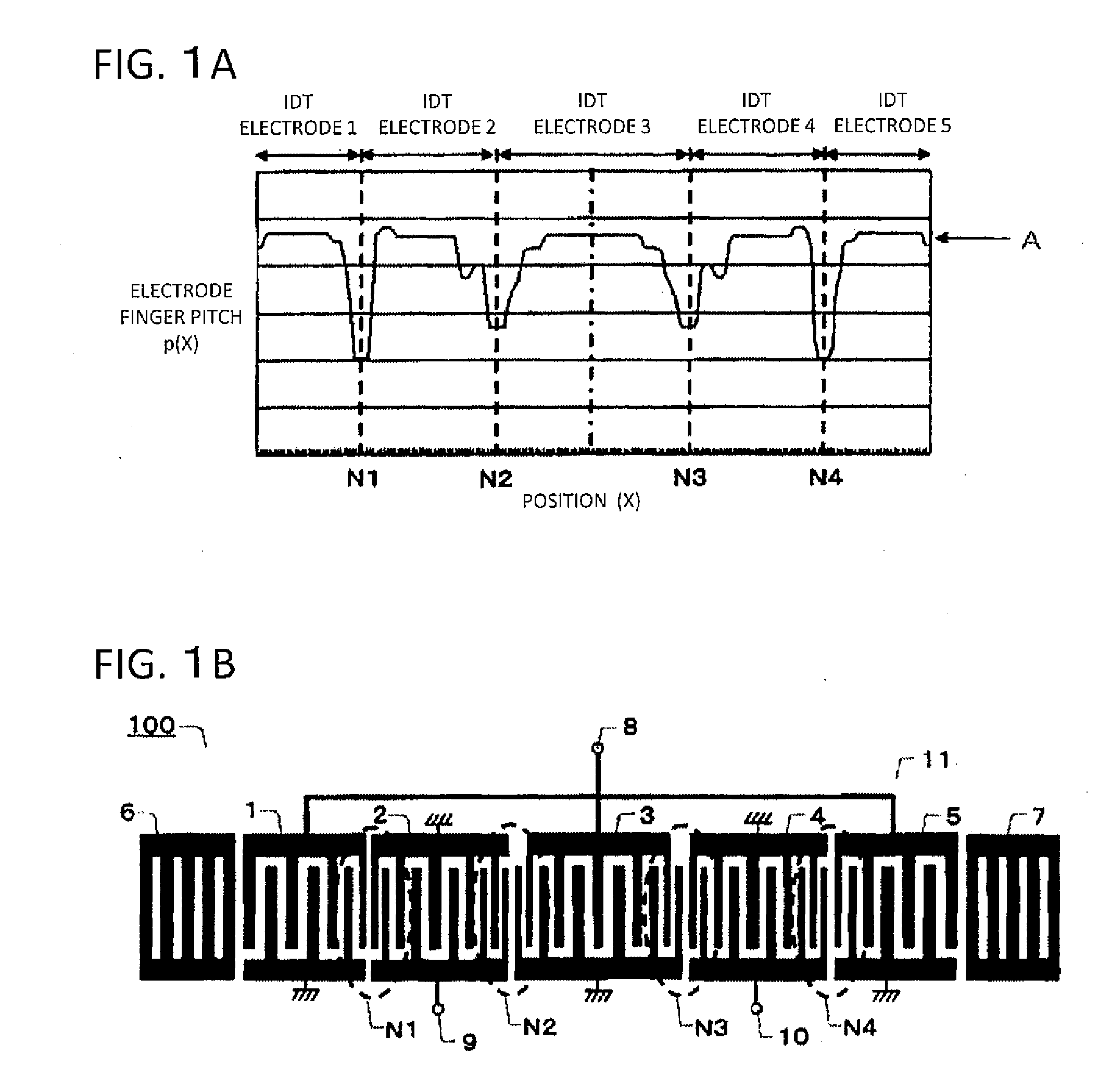
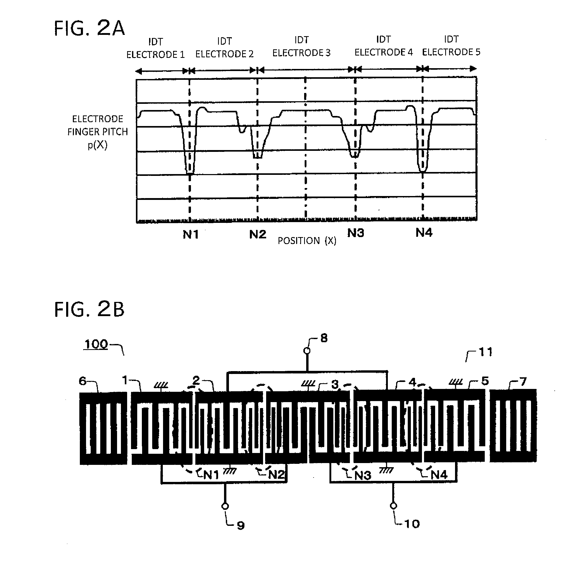
[0014]According to the SAW device of the present invention, in the low frequency region of the pass band, the electrode finger narrow pitch portions of the second and fourth IDT electrodes closer to the center among the five IDT electrodes are relatively wide, and the electrode finger narrow pitch portions of the first and fifth IDT electrodes on the reflector electrode sides are relatively narrow. Therefore, in the second and fourth IDT electrodes, at the position close to the center third IDT electrode, vibration of the SAW becomes strong. Along with this, vibration of the SAW at the third IDT electrode is weakened. Further, in the first and fifth IDT electrodes as well, vibration of the SAW becomes strong at the position close to the center third IDT electrode. Accordingly, by attenuation of vibration in the vicinity of the reflector electrodes, a reflection effect of the reflector electrodes becomes hard to obstruct. For this reason, the sharpness in the vicinity of the outside of the lower frequency side of the pass band can be improved.
[0015]Further, the first to fourth electrode finger narrow pitch portions having narrow electrode finger pitches are respectively formed at adjoining portions of the first to fifth IDT electrodes, an unbalanced input terminal or unbalanced output terminal and a balanced output terminal or balanced input terminal are connected to the SAW element, the electrode finger pitches of the first to fourth electrode finger narrow pitch portions are formed symmetrically with respect to the third IDT electrode located at the center, the electrode finger pitch of the second electrode finger narrow pitch portion is narrower than the electrode finger pitch of the first electrode finger narrow pitch portion, and the electrode finger pitch of the third electrode finger narrow pitch portion is narrower than the electrode finger pitch of the fourth electrode finger narrow pitch portion, whereby a propagation loss due to that the propagation length of the SAW becoming long is suppressed and the insertion loss can be suppressed.
[0016]Further, the first to fourth electrode finger narrow pitch portions having narrow electrode finger pitches are respectively formed at adjoining portions of the first to fifth IDT electrodes, therefore a balance type SAW filter can be realized in which conversion of a SAW to a bulk wave at the adjoining portions of the IDT electrodes can be effectively suppressed, insertion loss in the pass band can be improved, and the frequency characteristic is enhanced.
[0017]The communication device of the present invention is provided with at least one of a reception circuit and a transmission circuit which has any of the SAW devices of the present invention described above, whereby a device able to realize a frequency characteristic satisfying the severe conventional demands for insertion loss and sharpness is obtained, and a communication device having a reduced power consumption and much better sensitivity can be realized.

Problems solved by technology

For this reason, it has become difficult to sufficiently obtain the gain of an antenna.
Contrary to this, “unbalanced input” or “unbalanced output” means that a signal is input or output as a potential of one line with respect to a ground potential.

Method used


Image

  • Surface Acoustic Wave Device and Communication Device
  • Surface Acoustic Wave Device and Communication Device
  • Surface Acoustic Wave Device and Communication Device

Examples


embodiment 1

[0061]An embodiment of a SAW device of the present invention will be explained below.

[0062]An embodiment of preparing a SAW device having electrode finger pitches indicated by a solid line in FIG. 5A will be explained specifically. The SAW device of the present embodiment has, as shown in FIG. 5B, a constitution in which a SAW resonator 12 is connected between a SAW element 11 and an unbalanced signal terminal 8.

[0063]On the piezoelectric substrate (mother board for providing many units) 100 composed of a 38.7° Y-cut and X-direction propagation LiTaO3 single crystal, fine electrode patterns for various types of electrodes composed of Al (99 vol %)-Cu (1 vol %) alloy were formed.

[0064]Further, the electrodes were patterned by a photolithography method using a sputtering apparatus, a reduced projection exposure apparatus (stepper), and an RIE (reactive ion etching) apparatus.

[0065]First, the piezoelectric substrate 100 was ultrasonically cleaned by acetone, IPA (isopropyl alcohol), or...


PUM


Abstract

To provide a communication apparatus and a SAW device wherein the steepness in the vicinity of the outside of the lower frequencies of a passband can be improved. On a piezoelectric board 100, a SAW element 11 is formed which has first to fifth IDT electrodes 1-5 and reflector electrodes 6,7 with first to fourth electrode-finger narrow-pitch portions N1-N4 being formed in the respective ones of adjoining portions of the respective first to fifth IDT electrodes 1-5. An unbalanced signal terminal 8 and balanced signal terminals 9,10 are connected to the SAW element 11. The electrode finger pitches of the first to fourth electrode-finger narrow-pitch portions N1-N4 are formed symmetrically with respect to the third central IDT electrode 3 in such a manner that the electrode finger pitch of the first electrode-finger narrow-pitch portion N1 is narrower than that of the second electrode-finger narrow-pitch portion N2, while the electrode finger pitch of the fourth electrode-finger narrow-pitch portion N4 is narrower than that of the third electrode-finger narrow-pitch portion N3.

Description

TECHNICAL FIELD[0001]The present invention relates to a surface acoustic wave device, such as a surface acoustic wave filter, a surface acoustic wave resonator, or the like, used in, for example, a mobile phone or other mobile communication devices and to a communication device provided with the same.[0002]Note that, below, “surface acoustic wave” may be abbreviated as “SAW”.BACKGROUND ART[0003]Conventionally, as a frequency selection filter (below, also referred to as a “filter”) used in an RF (radio frequency) stage of a mobile phone, car phone, or other mobile communication devices, a SAW filter has been widely used. In general, the characteristics required for a frequency selection filter include a broad pass band, low loss, high amount of attenuation, and others. In recent years, particularly for improvement of reception sensitivity and lowering of power consumption in mobile communication devices, there have been rising demands for reduction of loss in SAW filters. Further, in...

Claims


Application Information

Patent Timeline
Patent Type & Authority Applications(United States)
IPC IPC(8): H03H9/25
CPCH03H9/0038H03H9/1457H03H9/14535
Inventor NAKAI, TSUYOSHI
Owner KYOCERA CORP
Learn More