Interconnection structure design for low RC delay and leakage

a technology of interconnection structure and leakage current, which is applied in the direction of semiconductor devices, semiconductor/solid-state device details, electrical apparatus, etc., can solve the problems of affecting the performance and reliability of fabricated circuits, the interconnection structure of fig. 1 suffers drawbacks, and the rc delay of the integrated circuit increases. , to achieve the effect of reducing rc delay, reducing leakage current, and reducing power consumption

Active Publication Date: 2013-04-30
ADVANCED MFG INNOVATIONS INC
View PDF6 Cites 14 Cited by
  • Summary
  • Abstract
  • Description
  • Claims
  • Application Information

AI Technical Summary

Benefits of technology

[0013]The advantageous features of the present invention include reduced RC delay, reduced leakage currents between interconnection lines, and less power consumption.

Problems solved by technology

The quality of the interconnection structure drastically affects the performance and reliability of the fabricated circuit.
The interconnection structure of FIG. 1 suffers drawbacks, however.
As a result, the RC delay of the integrated circuits increases.
Additionally, with a smaller spacing S between the metal lines, leakage current may become significant.
Besides, lowering the k value of inter-metal dielectric layer 108 is accompanied by the side effects of weaker mechanical properties and higher vulnerability to the “poisoning” of process chemicals.

Method used


Image

  • Interconnection structure design for low RC delay and leakage
  • Interconnection structure design for low RC delay and leakage
  • Interconnection structure design for low RC delay and leakage

Examples


Embodiment Construction

[0022]The making and using of the presently preferred embodiments are discussed in detail below. It should be appreciated, however, that the present invention provides many applicable inventive concepts that can be embodied in a wide variety of specific contexts. The specific embodiments discussed are merely illustrative of specific ways to make and use the invention, and do not limit the scope of the invention.

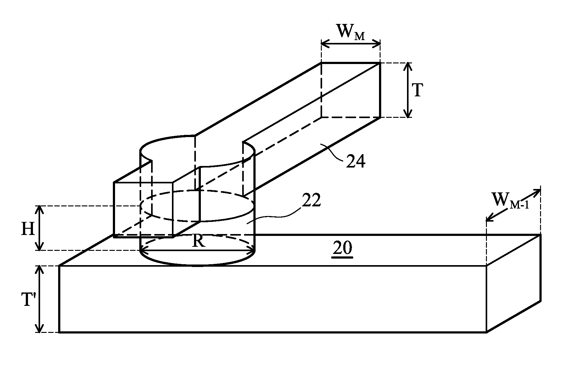
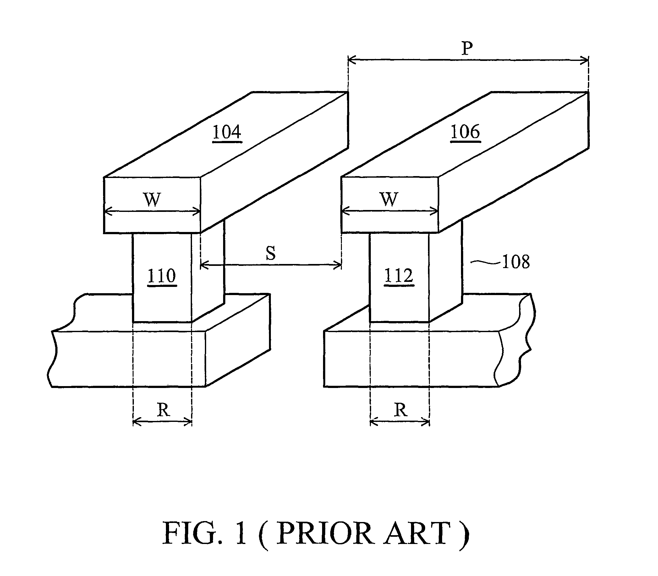
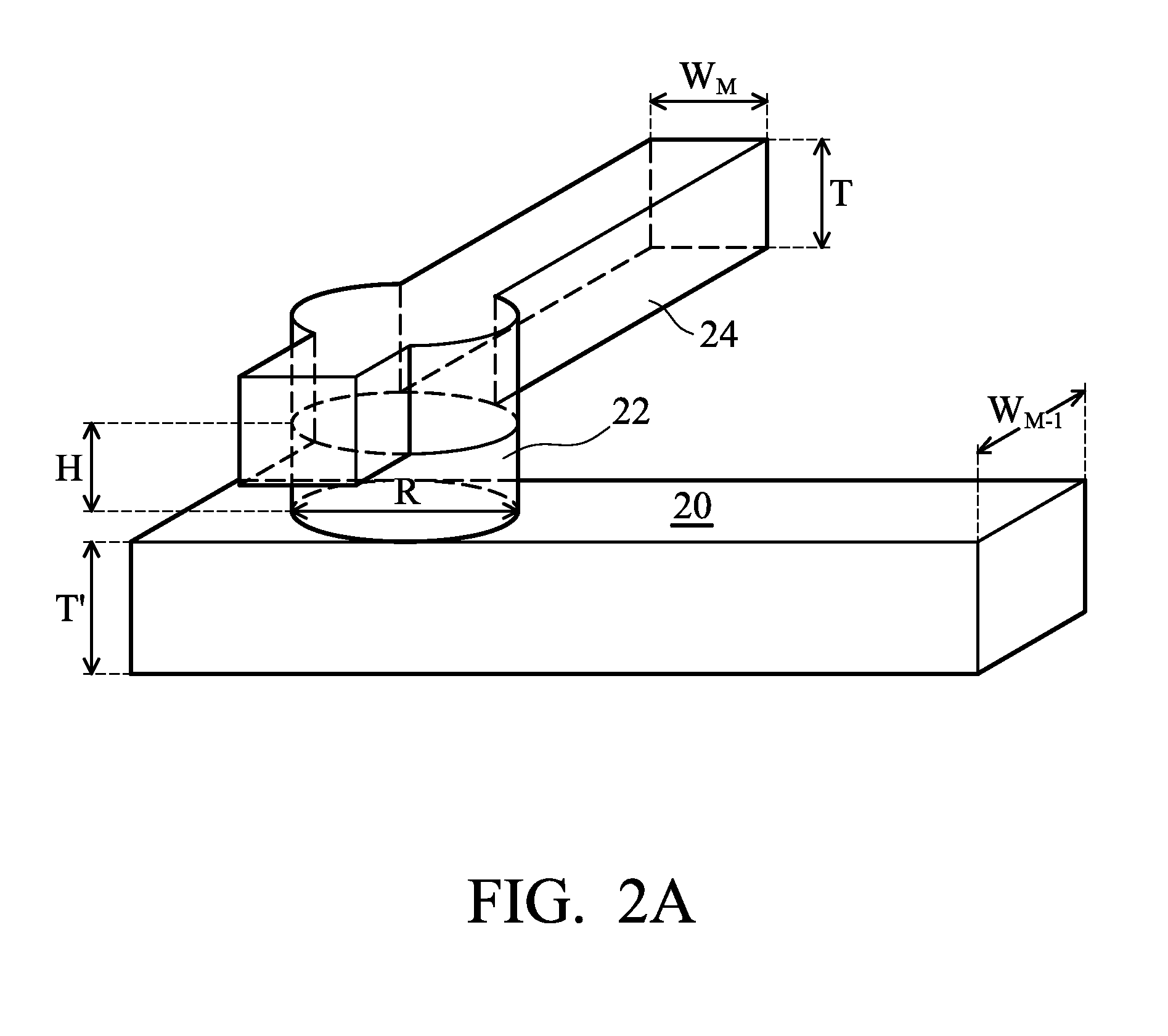
[0023]A novel interconnection structure is illustrated. Throughout the various views and illustrative embodiments of the present invention, like reference numbers are used to designate like elements. Although the preferred embodiments of the present invention are related to the design of interconnection structures concerning vias and metal lines, the same concept is readily available to the design of contact plugs and overlying metal lines, provided the reduced width metal lines are adequate for carrying the currents.

[0024]A perspective view of a preferred embodiment of the p...


PUM


Abstract

An interconnection structure for integrated circuits having reduced RC delay and leakage is provided. The interconnection structure includes a first conductive line in a first dielectric layer, a second dielectric layer over the first dielectric layer and the first conductive line, and a dual damascene structure in the second dielectric layer. The dual damascene structure includes a second conductive line and a via between and adjoining the first and the second conductive lines, wherein the second conductive line comprises a first portion directly over and adjoining the via, and a second portion having no underlying and adjoining vias. The second portion has a second width less than a first width of the first portion.

Description

TECHNICAL FIELD[0001]This invention relates generally to the formation of interconnection structures in integrated circuits, and more particularly to the layout of metal lines in metallization layers and connecting vias.BACKGROUND[0002]Modern integrated circuits are made up of literally millions of active devices such as transistors and capacitors. These devices are initially isolated from one another but are later interconnected together to form functional circuits. Typical interconnection structures include lateral interconnections, such as metal lines (wirings), and vertical interconnections, such as vias and contacts. The quality of the interconnection structure drastically affects the performance and reliability of the fabricated circuit. Interconnections are increasingly determining the limits of performance and the density of modern integrated circuits.[0003]FIG. 1 is a cross-sectional illustration of a conventional interconnection structure used in the semiconductor industry...

Claims


Application Information

Patent Timeline
Patent Type & Authority Patents(United States)
IPC IPC(8): H01L29/41
CPCH01L21/76807H01L21/76816H01L23/5226H01L23/528H01L2924/0002H01L2924/00
Inventor YU, CHEN-HUAYEH, MING-SHIH
Owner ADVANCED MFG INNOVATIONS INC
Why Eureka
Try Eureka