Memory formation with reduced metallization layers

a technology of metallization layer and memory, which is applied in the field of memory layout design and manufacturing methods, can solve the problems of high parasitic capacitance, high parasitic capacitance, and the drawbacks of conventional memory chip formation, and achieve the effects of reducing rc delay, reducing metallization layer, and reducing parasitic capacitan

Active Publication Date: 2009-04-07
MOSAID TECH
View PDF12 Cites 16 Cited by
  • Summary
  • Abstract
  • Description
  • Claims
  • Application Information

AI Technical Summary

Benefits of technology

[0008]The advantageous features of the present invention include reduced metallization layers for forming SRAM cells, reduced RC delay due to shortened contacts and full compatibility of the formation process of SRAM cells into the formation of DRAM cells.

Problems solved by technology

The conventional memory chip formation, however, suffers drawbacks.
Another drawback is that contact plugs connecting the source / drain regions of MOS devices in SRAM cells are tall contact plugs extending from M1 all the way down to source / drain regions of MOS devices.
The long contact plugs combined with the high device density of memory cells results in high parasitic capacitances.
RC delay is thus increased.

Method used


Image

  • Memory formation with reduced metallization layers
  • Memory formation with reduced metallization layers
  • Memory formation with reduced metallization layers

Examples


Embodiment Construction

[0017]The making and using of the presently preferred embodiments are discussed in detail below. It should be appreciated, however, that the present invention provides many applicable inventive concepts that can be embodied in a wide variety of specific contexts. The specific embodiments discussed are merely illustrative of specific ways to make and use the invention, and do not limit the scope of the invention.

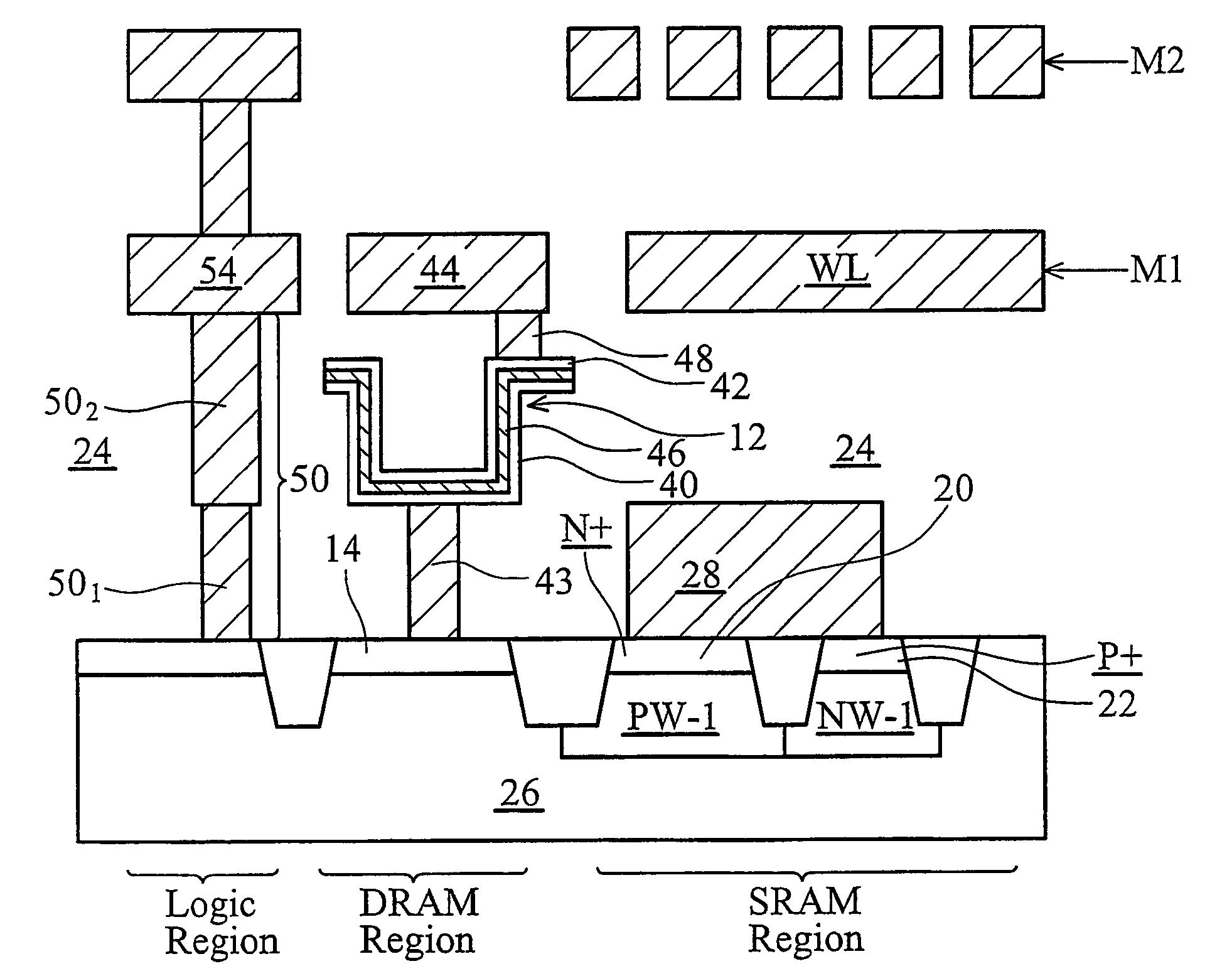
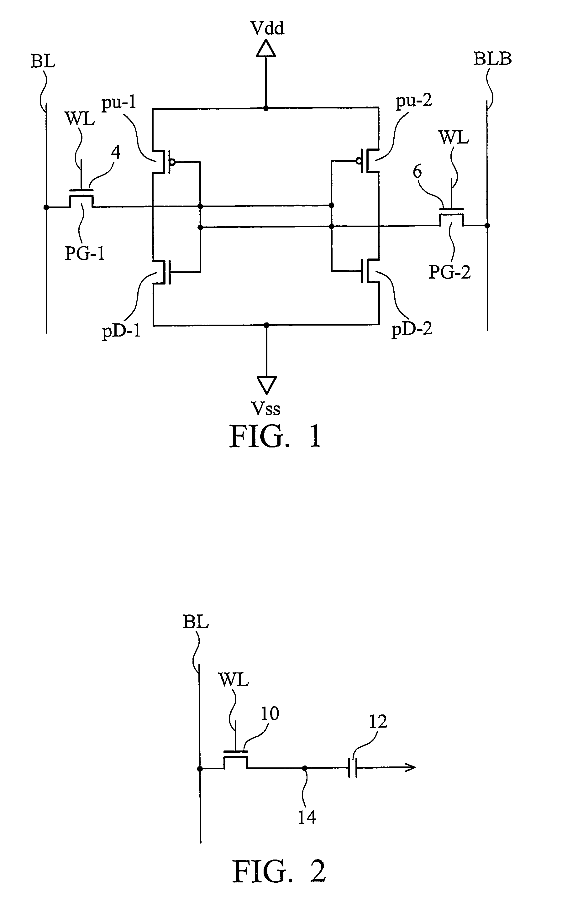
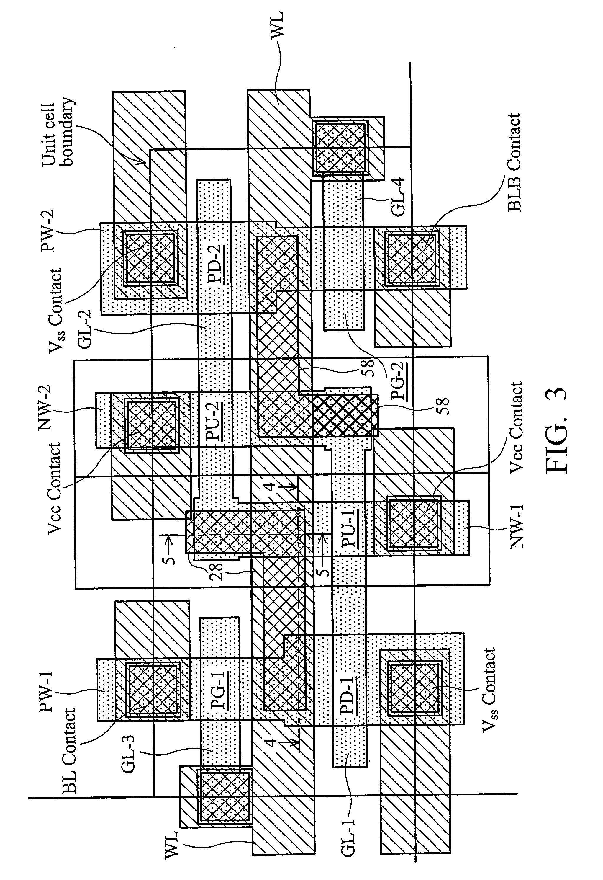
[0018]In the preferred embodiment, static random access memory (SRAM) cells and one-transistor (1T) dynamic random access memory (DRAM) cells are integrated on one chip. A chip thus includes at least a logic region for forming a logic circuit (such as a CPU, digital signal processing (DSP) unit, and the like), an SRAM region for forming an SRAM cell, and a DRAM region for forming a DRAM cell. For illustration purposes, throughout the description, a six-transistor (6T) SRAM cell and a 1T DRAM cell are discussed. It should be appreciated, however, that the teaching provided by ...


PUM


Abstract

A semiconductor structure includes a static random access memory (SRAM) cell comprising a first pull-up MOS device, a first pull-down MOS device and a first pass-gate MOS device, a first metallization layer, and an inter-layer dielectric (ILD) underlying the first metallization layer, wherein the ILD comprises an upper portion and a lower portion, a first first-layer contact in the lower portion of the ILD and connecting at least two of the first pull-up MOS device, the first pull-down MOS device and the first pass-gate MOS device. The first first-layer contact is physically isolated from second layer contacts in the upper portion of the ILD. The semiconductor structure further includes a second first-layer contact in the lower portion of the ILD, and a second-layer contact having at least a portion on the second first-layer contact, wherein the second layer contact electrically connects the second first-layer contact.

Description

TECHNICAL FIELD[0001]This invention relates generally to semiconductor devices, and more particularly to memories, and even more particularly to layout design and manufacturing methods of memories.BACKGROUND[0002]Static random access memory (SRAM) cells are popular for their high performance and low cost. In cache applications, particularly at L1 and L2 levels, six-transistor (6T) or eight-transistor (8T) SRAM cells are widely employed due to their high speed and process compatible cell structure. In applications requiring high storage amounts, however, for example, in L3 cache or memories with 32M bits or higher, one-transistor (1T) RAM cells with dynamic random access memory (DRAM) cells are preferred for their low chip area requirement. To achieve both high performance and high storage, SRAM and 1T DRAM memories are often integrated on one chip.[0003]The conventional memory chip formation, however, suffers drawbacks. Typically, the local interconnection in an SRAM cell, for examp...

Claims


Application Information

Patent Timeline
Patent Type & Authority Patents(United States)
IPC IPC(8): H01L27/088
CPCH01L27/105H01L27/10894H01L27/11H01L27/1104H01L27/1116H10B12/09H10B10/00H10B10/12H10B10/18
Inventor LIAW, JHON-JHY
Owner MOSAID TECH
Why Eureka
Try Eureka