Multi-layer printed circuit board and method of manufacturing multi-layer printed circuit board

a printed circuit board and multi-layer technology, applied in the direction of conductive pattern formation, insulating substrate metal adhesion improvement, electric connection formation of printed elements, etc., can solve the problems of deteriorating reliability of printed circuit board connection, inability to form fine through holes, and inability to meet the requirements of quality assurance, so as to shorten the time required for forming openings

Inactive Publication Date: 2005-02-24
IBIDEN CO LTD
View PDF25 Cites 105 Cited by
  • Summary
  • Abstract
  • Description
  • Claims
  • Application Information

AI Technical Summary

Benefits of technology

A printed circuit board and a method of manufacturing a printed circuit board claimed in claims 23 to 26 have a structure that the resin plate has openings formed by CO2 laser beams (YAG laser beams, excimer laser beams or UV laser beams). Therefore, penetrating openings each having a smaller diameter as compared with that of each of penetrating openings formed by drilling can be formed. As distinct from a structure that openings are formed in a copper-clad laminated board by laser beams, leaving of copper in the th

Problems solved by technology

Since the core substrate has a thickness of about 1 mm, fine through holes cannot, however, easily be formed.
Thus, satisfactory reliability cannot be obtained.
Thus, a fact has been detected that the reliability in the connection of the printed circuit board deteriorates owing to the air bubble and the non-filled portion.
Thus, the process takes a long time and the cost is enlarged.
A fact has, however, been detected that the BT resin board having a flat surface encounters deterioration in the adhesiveness with a metal film formed on the right side of the core substrate.
Thus, there arises problems in that the resin film, however, encounters decrease in the strength required for the core substrate and the interlayer resin insulating layer cannot be formed in the

Method used


Image

  • Multi-layer printed circuit board and method of manufacturing multi-layer printed circuit board
  • Multi-layer printed circuit board and method of manufacturing multi-layer printed circuit board
  • Multi-layer printed circuit board and method of manufacturing multi-layer printed circuit board

Examples


first embodiment

(Fourth Modification of First Embodiment)

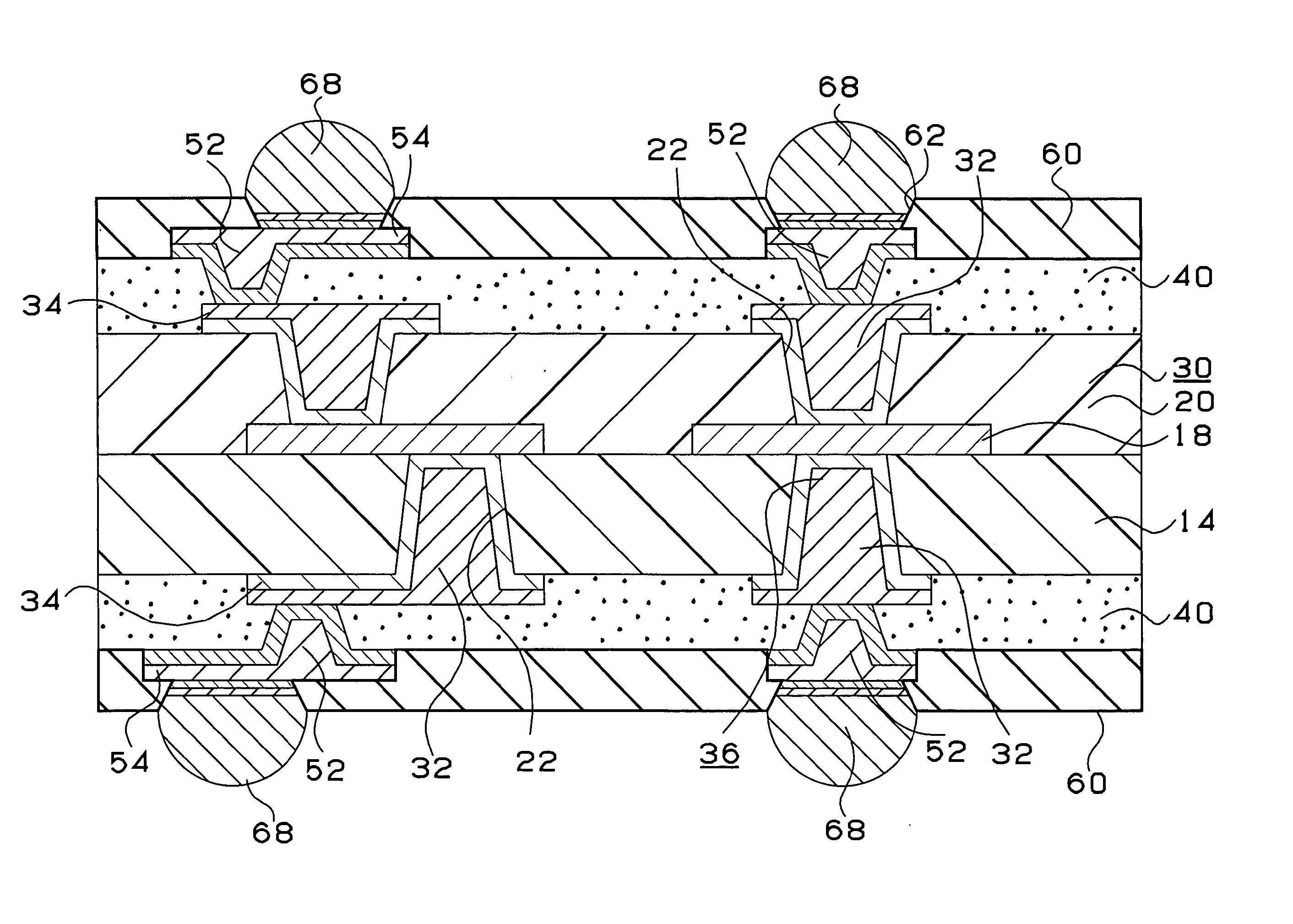
The structure of a multi-layer printed circuit board according to a fourth modification of the first embodiment will now be described with reference to FIG. 11.

The multi-layer printed circuit board according to the first embodiment described with reference to FIG. 6 incorporates the solder bumps 68 for connecting a daughter board, the solder bumps 68 being disposed on the lower surface of the multi-layer printed circuit board. On the other hand, the fourth modification incorporates conductive connection pins 78. Since the other structure is similar to that of the multi-layer printed circuit board described with reference to FIG. 6, the other structure is omitted from description.

[Second Embodiment]

The structure of the multi-layer printed circuit board according to a second embodiment of the present invention will now be described with reference to FIG. 18 which is a cross sectional view.

A multi-layer printed circuit board 210 accordin...

second embodiment

(Second Modification of Second Embodiment)

The cross section of a multi-layer printed circuit board according to a second modification is shown in FIG. 24. The structure of the second modification is similar to that according to the second embodiment. Note that the multi-layer printed circuit board according to the second modification has the structure that the interlayer resin insulating layer 250 and the interlayer resin insulating layer 281 are constituted by adhesive agent 257 for the upper layer and adhesive agent 255 for the lower layer each having the following composition. Moreover, coating in the liquid state is Performed, and then exposure and development were performed to form the openings.

A. Raw Material Composition for Preparing Adhesive Agent for Electroless Plating (Adhesive Agent for Upper Layer)

[Resin Composition (1)]

Mixing and stirring of 35 parts by weight of resin solution obtained by dissolving 25% acryl material of cresol novolac epoxy resin (manufactured ...

third embodiment

The third embodiment enables through holes each having a diameter of 100 μm or smaller can reliably be formed. Moreover, any air bubble is not formed and the interlayer resin insulating layer can be flattened. Therefore, the connection easiness and the reliability can be improved. When the interlayer material (the resin insulating layer) of the core substrate is made of the same material as that of the interlayer resin insulating layer, the layers does not easily separated. As a result, the reliability can furthermore be improved.

[Fourth Embodiment]

The structure of a multi-layer printed circuit board according to a fourth embodiment will now be described with reference to FIG. 46 which is across sectional view showing a multi-layer printed circuit board 410 serving as a package substrate and FIG. 47 showing a state in which an IC chip has been mounted so as to be joined to a daughter board.

As shown in FIG. 47, the multi-layer printed circuit board 410 incorporates a core substra...


PUM

PropertyMeasurementUnit
Thicknessaaaaaaaaaa
Diameteraaaaaaaaaa
Solubility (mass)aaaaaaaaaa

Abstract

A metal layer 18 is sandwiched between insulating layers 14 and 20 so that required strength is maintained. Hence it follows that the thickness of a core substrate 30 can be reduced and, therefore, the thickness of a multi-layer printed circuit board can be reduced. Formation of non-penetrating openings 22 which reach the metal layer 18 in the insulating layers 14 and 20 is simply required. Therefore, small non-penetrating openings 22 can easily be formed by applying laser beams. Thus, through holes 36 each having a small diameter can be formed.

Description

TECHNICAL FIELD The present invention relates to a multilayer printed circuit board which can be employed as a package substrate on which electronic elements, such as IC, are mounted. More particularly, the present invention relates to a multi-layer printed circuit board constituted by building interlayer resin insulating layers up on a core substrate and a method of manufacturing a multi-layer printed circuit board. BACKGROUND ART Hitherto, a buildup multi-layer printed circuit board has been manufactured by a method disclosed in Japanese Patent Laid-Open No. 9-130050. That is, an interlayer resin insulating layer is built on a core substrate having through holes formed therein. Then, a circuit pattern is formed on the interlayer resin insulating layer. The foregoing process is repeated so that the buildup multilayer printed circuit board is obtained. At present, the through holes are formed in the core substrate by forming penetrating openings by using a drill. Therefore, the ...

Claims


Application Information

Patent Timeline
IPC IPC(8): H01L21/48H01L23/498H05K1/03H05K3/00H05K3/10H05K3/18H05K3/38H05K3/42H05K3/46
CPCH05K3/181Y10T29/49155H05K3/385H05K3/387H05K3/388H05K3/423H05K3/426H05K3/427H05K3/4602H05K2201/0195H05K2201/0352H05K2201/0355H05K2201/0394H05K2201/09536H05K2201/09563H05K2201/0959H05K2201/096H05K2201/09736H05K2201/09881H05K2203/0315H05K2203/0733H05K2203/0773H05K2203/1476H01L21/486H01L23/49822H01L23/49827H01L2224/16H01L2924/0102H01L2924/01046H01L2924/01078H01L2924/01079H01L2924/15174H01L2924/15311H01L2924/15312H05K1/036H05K3/0032H05K3/0035H05K3/0038H05K3/108H01L2924/01019H01L2924/01087H01L2224/16235Y10T29/49165Y10T29/49144Y10T29/49126H05K3/381H01L2224/05568H01L2224/05573H01L2224/16225H01L2924/00014H01L2224/05599
Inventor ASAI, MOTOOWANG, DONGDONGMORI, TAKAHIRO
Owner IBIDEN CO LTD
Why Eureka
Try Eureka