Nonvolatile memory device and method of fabricating the same

a non-volatile memory and memory device technology, applied in the direction of semiconductor devices, basic electric elements, electrical apparatus, etc., can solve the problems of insufficient guarantee of the coupling ratio of the cell transistor in the non-volatile memory device, the difficulty in performing subsequent processing steps, etc., to achieve the effect of reducing the program and erase voltage, and improving the program and erase speed

Inactive Publication Date: 2006-02-02
SAMSUNG ELECTRONICS CO LTD
View PDF7 Cites 104 Cited by
  • Summary
  • Abstract
  • Description
  • Claims
  • Application Information

AI Technical Summary

Benefits of technology

[0030] Therefore, the present invention provides a nonvolatile memory device for improving program and erase speeds while decreasing program and erase voltages, and a method of fabricating the same.
[0031] The present invention also provides a nonvolatile memory device for improving program and erase speeds while preventing degradation of a tunnel oxide layer, and a method of fabricating the same.
[0032] The present invention also provides a nonvolatile memory device for improving program and erase speeds while decreasing a leakage current of a tunnel oxide layer, and a method of fabricating the same.

Problems solved by technology

The stack structure of the nonvolatile memory device causes a high step height difference relative to a cell array region and peripheral circuit regions, thereby resulting in difficulties in performing subsequent processing steps.
Furthermore, since a process of patterning the floating gate is complicated, and the surface area of the floating gate is difficult to increase, a coupling ratio of the cell transistor in the nonvolatile memory device, which influences program and erase characteristics of the cell transistor, cannot be sufficiently ensured.
However, the process of increasing the surface area of the floating gate has many difficulties as the integration degree of the nonvolatile memory device is gradually increased.
Therefore, since it takes a long time to decrease the threshold voltage of the transistor, the time for data erasing is lengthened.
As described above, while the nonvolatile memory device has an advantage of storing data without power supply, it has a disadvantage of a low operation speed because the data program and erase are conducted by using a threshold voltage of the transistor, which is changed when electrons or holes are injected into the trapping layer, and injected electrons or holes are discharged out of the trapping layer.
However, the SONOS structure shown in FIG. 4 generates a high potential barrier between the control gate electrode and the blocking layer so as to decrease a possibility that electrons tunnel the blocking insulating layer, but cannot improve program and erase speeds of the transistor due to the leakage current of the tunnel oxide layer.
However, the increase of program and erase voltages may cause problems, such as degradation of the tunnel oxide layer, and malfunctions of endurance and data retention.

Method used


Image

  • Nonvolatile memory device and method of fabricating the same
  • Nonvolatile memory device and method of fabricating the same
  • Nonvolatile memory device and method of fabricating the same

Examples


Embodiment Construction

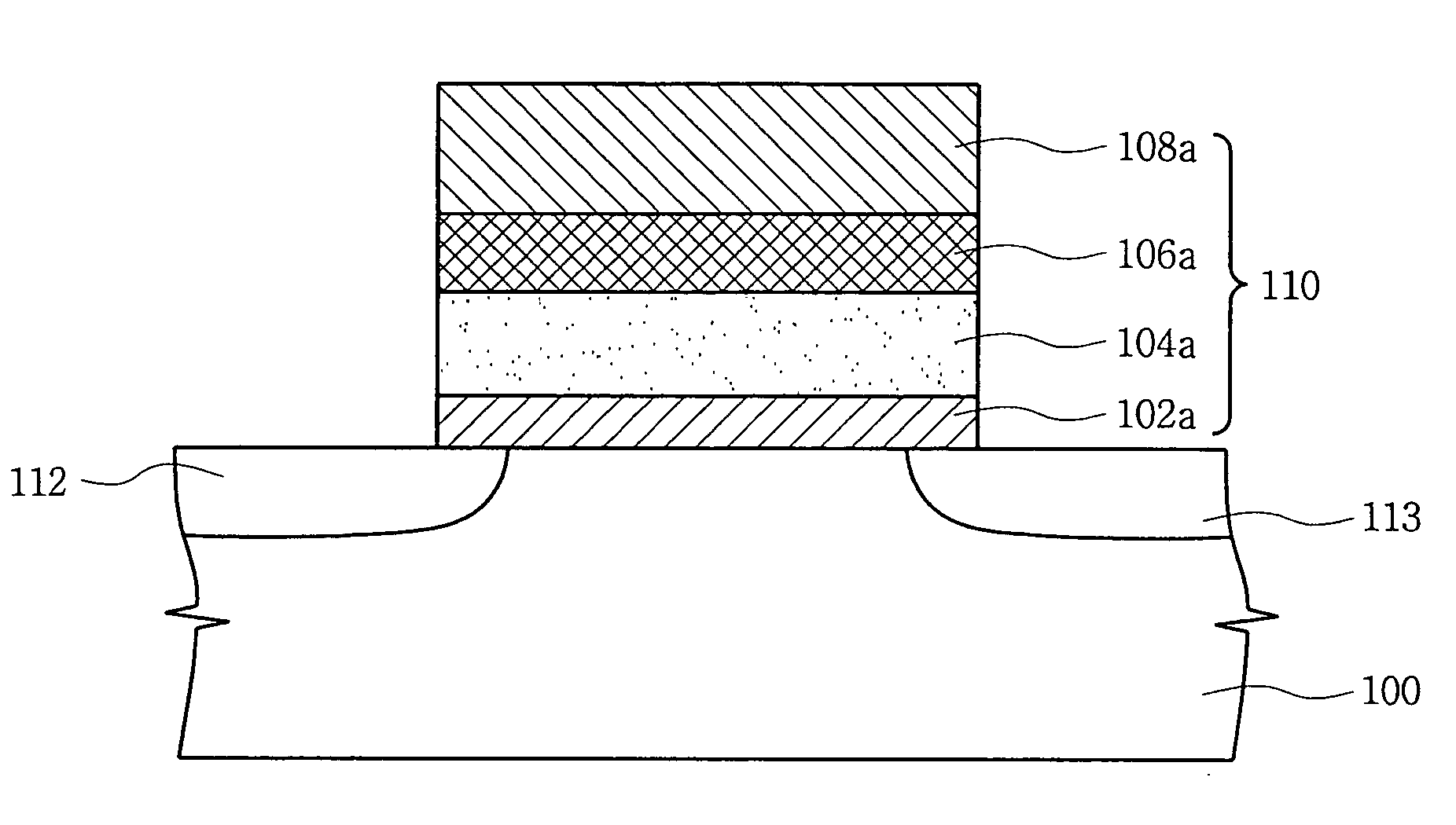
[0064]FIGS. 7A through 7B are sectional views illustrating a method of fabricating a nonvolatile memory device according to an embodiment of the present invention.

[0065] Referring to FIG. 7A, an insulating layer 102 is formed on a p-type semiconductor substrate 100, and the insulating layer 102 will function as a tunnel oxide layer for electron tunneling. The insulating layer 102 is composed of SiO or SION, and the material may be deposited using a chemical vapor deposition (CVD) method.

[0066] Then, a first high-k dielectric 104 is deposited on the insulating layer 102 to form a trapping layer functioning as a charge storage layer. The formation of the trapping layer using the high-k dielectric 104 is one of the features of the present invention, and the first high-k dielectric 104 is preferably deposited using an atomic layer deposition (ALD) or CVD method. The first high-k dielectric 104 is formed of a metal oxide layer, and may be composed of a material selected from HfO, HfON,...


PUM


Abstract

There are provided a nonvolatile memory device and a method of fabricating the same. A gate region of the nonvolatile memory device is formed as a stack structure including a tunnel oxide layer, a trapping layer, a blocking layer and a control gate electrode. The trapping layer is formed of a high-k dielectric having a higher dielectric constant than that of the tunnel oxide layer. When the trapping layer is formed of high-k dielectric, an EOT in a same thickness can be reduced, and excitation of electrons of the control gate electrode to the tunnel oxide layer due to a high potential barrier relative to the tunnel oxide layer is prevented so that program and erase voltages can be further reduced. As such, a problem that the tunnel oxide layer is damaged due to the conventional high program and erase voltages can be solved by reducing the program and erase voltages, and program and erase speeds of the transistor can be further improved.

Description

CROSS-REFERENCE TO RELATED APPLICATION [0001] This application claims the benefit of Korean Patent Application No. 10-2004-0060338, filed Jul. 30, 2004, the contents of which are hereby incorporated herein by reference in their entirety. BACKGROUND OF THE INVENTION [0002] 1. Technical Field [0003] The present invention relates to a nonvolatile memory device and a method of fabricating the same, and, more particularly, to a nonvolatile memory device having an improved gate structure for improving program and erase speeds, and a method of fabricating the same. [0004] 2. Discussion of Related Art [0005] Generally, semiconductor memory devices used to store data are classified as volatile memory devices and nonvolatile memory devices. While the volatile memory device loses stored data when power supply is removed, the nonvolatile memory device retains stored data even though power supply is removed. Therefore, the nonvolatile memory device can be widely used for memory cards to store mu...

Claims


Application Information

Patent Timeline
Patent Type & Authority Applications(United States)
IPC IPC(8): H01L29/76
CPCH01L29/792H01L29/513
Inventor DOH, SEOK-JOOKIM, JONG-PYOLEE, JONG-HOKIM, KI-CHUL
Owner SAMSUNG ELECTRONICS CO LTD
Why Eureka
Try Eureka