OLED display panel

一种显示面板、显示区的技术,应用在OLED显示面板领域,能够解决颜色偏差、数据信号电压偏差、显示画面亮度偏差等问题,达到亮度正常且无色偏、避免亮度偏差或颜色偏差的效果

Inactive Publication Date: 2019-12-31
WUHAN CHINA STAR OPTOELECTRONICS SEMICON DISPLAY TECH CO LTD
View PDF3 Cites 2 Cited by
  • Summary
  • Abstract
  • Description
  • Claims
  • Application Information

AI Technical Summary

Problems solved by technology

However, in actual situations, there is a voltage drop in the vertical direction of the driving voltage lines 60 ′, that is, each driving voltage line 60 ′ provides a driving voltage for a column of sub-pixels 10 ′, and the pixel driving current will flow through the driving voltage lines 60 ′. There is resistance in the voltage line 60' itself, so the driving voltage corresponding to a column of sub-pixels 10' will gradually decrease along the vertical direction, resulting in a certain deviation in the voltage of the data signal actually written into the pixel driving circuit, which in turn causes the display screen Have brightness deviation or color deviation
In addition, a plurality of driving voltage lines 60' are connected through a driving voltage connecting line 61' extending in the horizontal direction, so there is also a voltage drop in the driving voltage in the horizontal direction.
The driving voltage connection line 61' is arranged in the non-display area of ​​the OLED display panel. In order to minimize the voltage drop in the horizontal direction and reduce the resistance of the driving voltage connection line 61', it is necessary to use a wider driving voltage connection line 61'. This layout is not conducive to the design of narrow bezel displays

Method used


Image

  • OLED display panel
  • OLED display panel
  • OLED display panel

Examples


Embodiment Construction

[0031] In order to further illustrate the technical means adopted by the present invention and its effects, the following describes in detail in conjunction with preferred embodiments of the present invention and accompanying drawings.

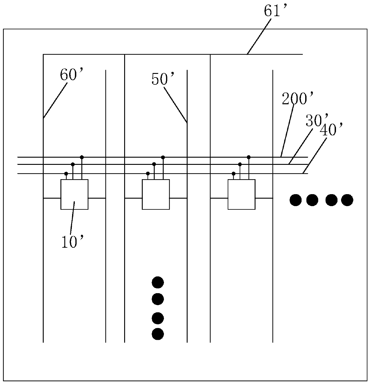
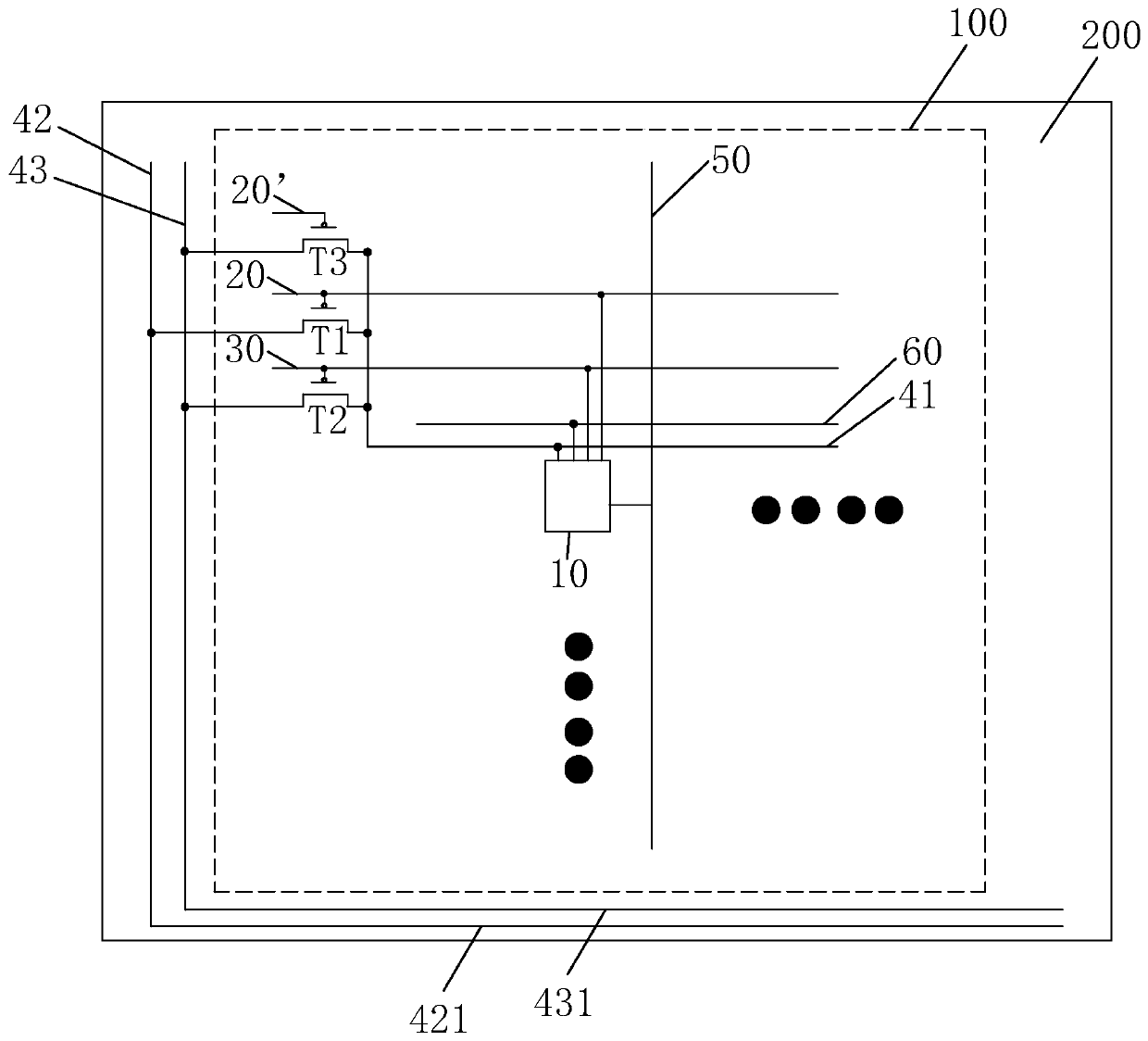
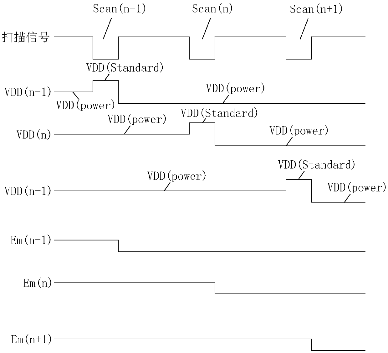
[0032] see figure 2 and image 3 , the present invention provides an OLED display panel, comprising: a plurality of sub-pixels 10 arranged in an array, a plurality of scanning signal lines 20 extending in the horizontal direction, a plurality of light-emitting signal lines 30 and a plurality of first driving voltage lines 41, And a plurality of data signal lines 50 extending vertically, at least one second driving voltage line 42 and at least one third driving voltage line 43;

[0033] Each scanning signal line 20 is correspondingly connected to a row of sub-pixels 10, each light emitting signal line 30 is correspondingly connected to a row of sub-pixels 10, each first driving voltage line 41 is correspondingly connected to a row of sub-pixe...


PUM


Abstract

The invention provides an OLED display panel. The OLED display panel comprises a plurality of sub-pixels arranged in an array, a plurality of scanning signal lines, a plurality of light-emitting signal lines, a plurality of first driving voltage lines, a plurality of data signal lines, at least one second driving voltage line and at least one third driving voltage line, wherein the scanning signallines, the light-emitting signal lines and the first driving voltage lines extend in the horizontal direction, and the data signal lines, the second driving voltage lines and the third driving voltage lines extend in the vertical direction, wherein each scanning signal line is connected with a row of sub-pixels, each light-emitting signal line is connected with a row of sub-pixels, each first driving voltage line is connected with a row of sub-pixels, and each data signal line is connected with a column of sub-pixels; the first driving voltage line corresponding to each row of sub-pixels is connected with the second driving voltage line through a first thin film transistor; and the first driving voltage line corresponding to each row of sub-pixels is connected with the third driving voltage line through a second thin film transistor, so that brightness deviation or color deviation of the sub-pixels during light emitting can be avoided.

Description

technical field [0001] The invention relates to the field of display technology, in particular to an OLED display panel. Background technique [0002] Organic Light Emitting Display (OLED) display panel, referred to as OLED panel, has self-illumination, low driving voltage, high luminous efficiency, short response time, high definition and contrast, nearly 180° viewing angle, and wide operating temperature range. It can realize many advantages such as flexible display and large-area full-color display, and is recognized by the industry as a display device with the most development potential. [0003] The OLED is a current-driven device. When a current flows through the OLED, the OLED emits light, and the brightness of the light is determined by the current flowing through the OLED itself. Such as figure 1 As shown, the existing OLED display panel includes: a plurality of sub-pixels 10' arranged in an array, a plurality of scanning signal lines 200' extending in the horizon...

Claims


Application Information

Patent Timeline
Patent Type & Authority Applications(China)
IPC IPC(8): G09G3/3208G09G3/3266
CPCG09G3/3208G09G3/3266G09G2300/0426G09G2300/0861G09G2320/0219G09G2310/0251G09G2310/0262G09G2320/0223G09G3/3233G09G3/3258G09G3/3291
Inventor 王威黄情
Owner WUHAN CHINA STAR OPTOELECTRONICS SEMICON DISPLAY TECH CO LTD
Why Eureka
Try Eureka