Organic electroluminescent display and method of manufacturing the same

a technology of electroluminescent display and electroluminescent display, which is applied in the direction of discharge tube luminescnet display, discharge tube/lamp details, electric discharge lamps, etc., can solve the problems of increasing the line resistance of a cathode, the brightness of an image is not uniform, and the external efficiency of the electroluminescent display is lower than that of other displays such as cathode-ray tubes and plasma display panels. achieve the effect of reducing the line resistance of an electrod

Active Publication Date: 2005-07-12
SAMSUNG DISPLAY CO LTD
View PDF7 Cites 18 Cited by
  • Summary
  • Abstract
  • Description
  • Claims
  • Application Information

AI Technical Summary

Benefits of technology

[0011]The present invention provides an organic electroluminescent display for reducing the line resistance of an electrode so that the brightness of an image can be prevented from being nonuniform due to the line resistance.

Problems solved by technology

Organic electroluminescent displays have lower external efficiency than other displays such as cathode-ray tubes and plasma display panels (PDPs).
In the meantime, in organic electroluminescent displays having the above-described structure, as the size of a panel increases, the line resistance of an electrode increases, which causes the brightness of an image to be nonuniform.
In particular, when an organic electroluminescent display is driven by a thin-film transistor, the line resistance of a cathode increases, and thus the above problem occurs.
These conventional organic electroluminescent displays are not provided with an element for reducing the line resistance of a cathode and thus still have a problem of nonuniform brightness of an image due to the line resistance.

Method used


Image

  • Organic electroluminescent display and method of manufacturing the same
  • Organic electroluminescent display and method of manufacturing the same
  • Organic electroluminescent display and method of manufacturing the same

Examples


Embodiment Construction

[0018]Reference will now be made in detail to the embodiments of the present invention, examples of which are illustrated in the accompanying drawings, wherein like reference numerals refer to the like elements throughout. The embodiments are described below in order to explain the present invention by referring to the figures.

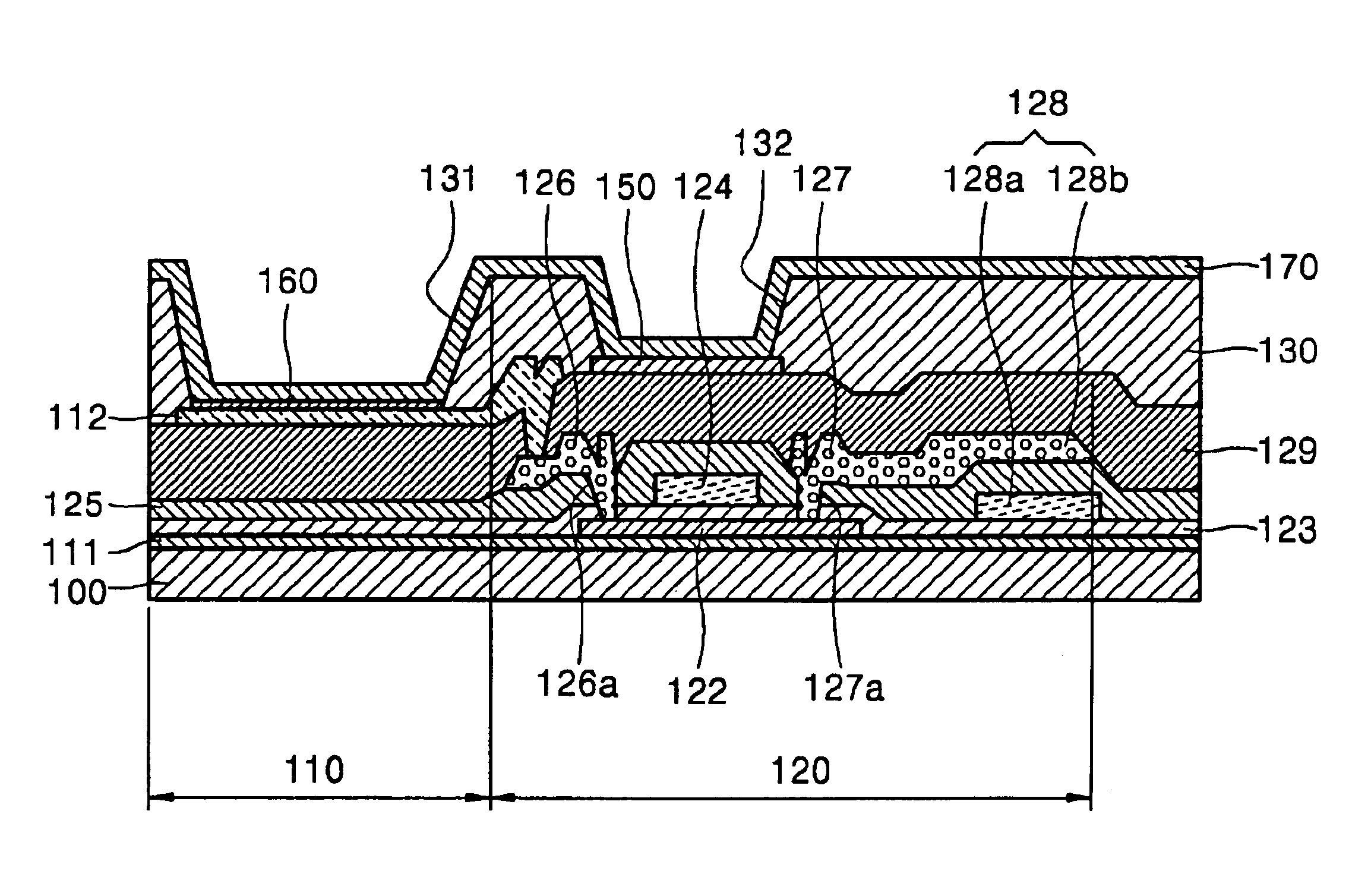
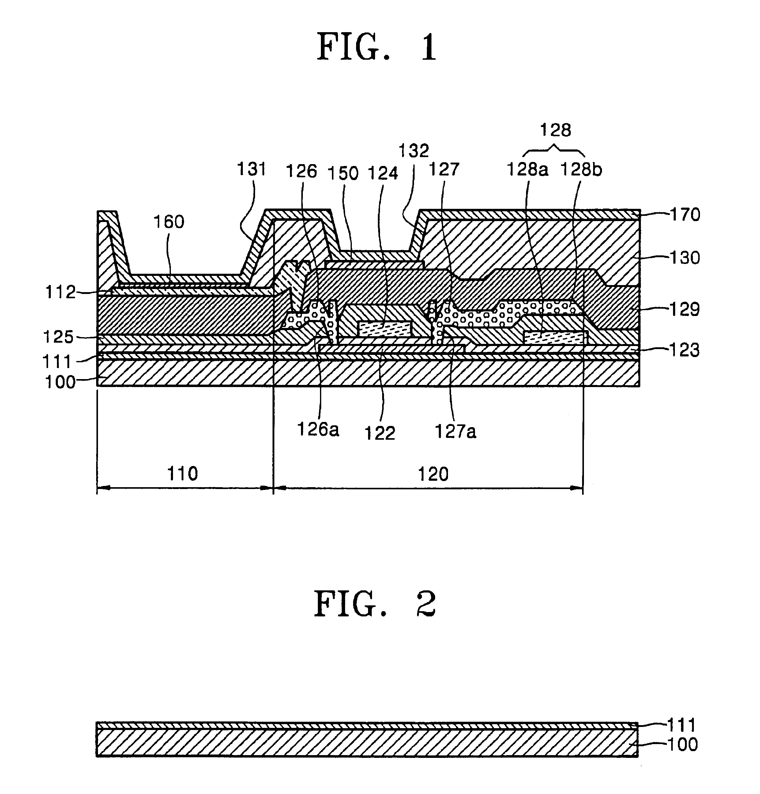
[0019]FIG. 1 shows an example of an active matrix organic light emitting display (AMOLED), as an organic electroluminescent display according to an embodiment of the present invention. Referring to FIG. 1, a buffer layer 111 is formed on a top surface of a transparent substrate 100. The organic electroluminescent display shown in FIG. 1 is largely divided into a pixel formation section 110, which includes a first electrode 112 for forming a pixel above the buffer layer 111, and a driving section 120, which drive electrodes of the pixel formation section 110 using thin-film transistors (TFTs) and capacitors.

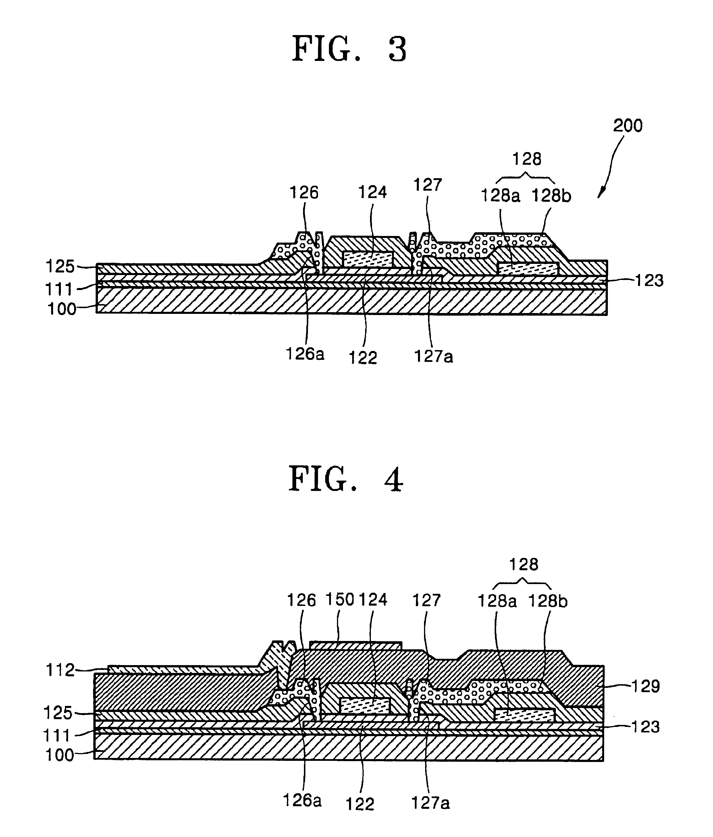
[0020]The driving section 120 includes TFTs and capaci...


PUM


Abstract

An organic electroluminescent display and a method of manufacturing the same are provided. The organic electroluminescent display includes a substrate, at least a thin-film transistor, which is formed on the substrate, at least an insulation layer, which cover the thin-film transistor, first electrodes, which are formed in a predetermined pattern on a top surface of the insulation layer and to which a voltage is selectively applied through the thin-film transistor, bus electrodes, which are insulated from the first electrodes, a planarization layer, which is an insulation layer and has openings exposing the first electrodes and the bus electrodes, organic layers, which are formed on a top surface of the first electrodes, and second electrodes, which are formed on a top surface of the organic layer and a top surface of the planarization layer and are electrically connected to the bus electrodes.

Description

CROSS-REFERENCE TO RELATED APPLICATIONS[0001]This application claims the priority of Korean Patent Application No. 2002-57336, filed on Sep. 19, 2002, in the Korean Intellectual Property Office, the disclosure of which is incorporated herein in by reference.BACKGROUND OF THE INVENTION[0002]1. Field of the Invention[0003]The present invention relates to an organic electroluminescent display, and more particularly, to an organic electroluminescent display with an improved electrode structure.[0004]2. Description of the Related Art[0005]Generally, organic electroluminescent displays are self-luminescent displays which emit light by electrically exciting a fluorescent organic compound. They can be operated with low voltage and can be made thin. In addition, organic electroluminescent displays have advantages, such as a wide viewing angle and a fast response speed, that overcome the problems of liquid crystal displays. Accordingly, they have been noted as next generation displays.[0006]I...

Claims


Application Information

Patent Timeline
Patent Type & Authority Patents(United States)
IPC IPC(8): H05B33/26H01L27/32H01L51/50H05B33/10H05B33/22
CPCH01L27/3244H01L51/5221H01L51/5228H05B33/26H01L27/3246H01L51/56H10K59/122H10K59/12H10K50/824H10K71/00
Inventor KOO, JAE-BONPARK, SANG-IL
Owner SAMSUNG DISPLAY CO LTD
Why Eureka
Try Eureka