Touch panel and method for manufacturing the same

a technology of touch panel and manufacturing method, which is applied in the direction of superimposed coating process, liquid/solution decomposition chemical coating, instruments, etc., can solve the problems of scratch generation, deformation of the performance of the resistive touch panel, etc., and achieve the effect of reducing the resistance of the connection part, reducing the resistance of the first electrode and/or the second electrode, and improving the electric stability and touch sensitivity

Inactive Publication Date: 2013-07-18
LG INNOTEK CO LTD
View PDF6 Cites 19 Cited by
  • Summary
  • Abstract
  • Description
  • Claims
  • Application Information

AI Technical Summary

Benefits of technology

[0010]According to the touch panel of the embodiment, resistance of the connection part is lower than resistance of the sensor part, so that resistance of the first electrode and / or the second electrode is lowered, thereby improving the electric stability and touch sensitivity.
[0011]According to the touch panel of another embodiment, the connection part includes a nano wire or carbon nano tube, so superior optical and electric characteristics can be obtained. In detail, the transmittance and transparent degree of the touch panel can be improved while lowering resistance.
[0012]According to the method for manufacturing the touch panel of the embodiment, the connection part is formed through the printing process, so that the manufacturing process can be simplified. Since the connection part of the first electrode, the insulating layer and the connection part of the second electrode are sequentially formed through the printing process, the manufacturing process can be more simplified.

Problems solved by technology

The performance of the resistive touch panel may be degraded if the resistive touch panel is repeatedly used for a long time, and scratch may be generated.

Method used


Image

  • Touch panel and method for manufacturing the same
  • Touch panel and method for manufacturing the same
  • Touch panel and method for manufacturing the same

Examples


second embodiment

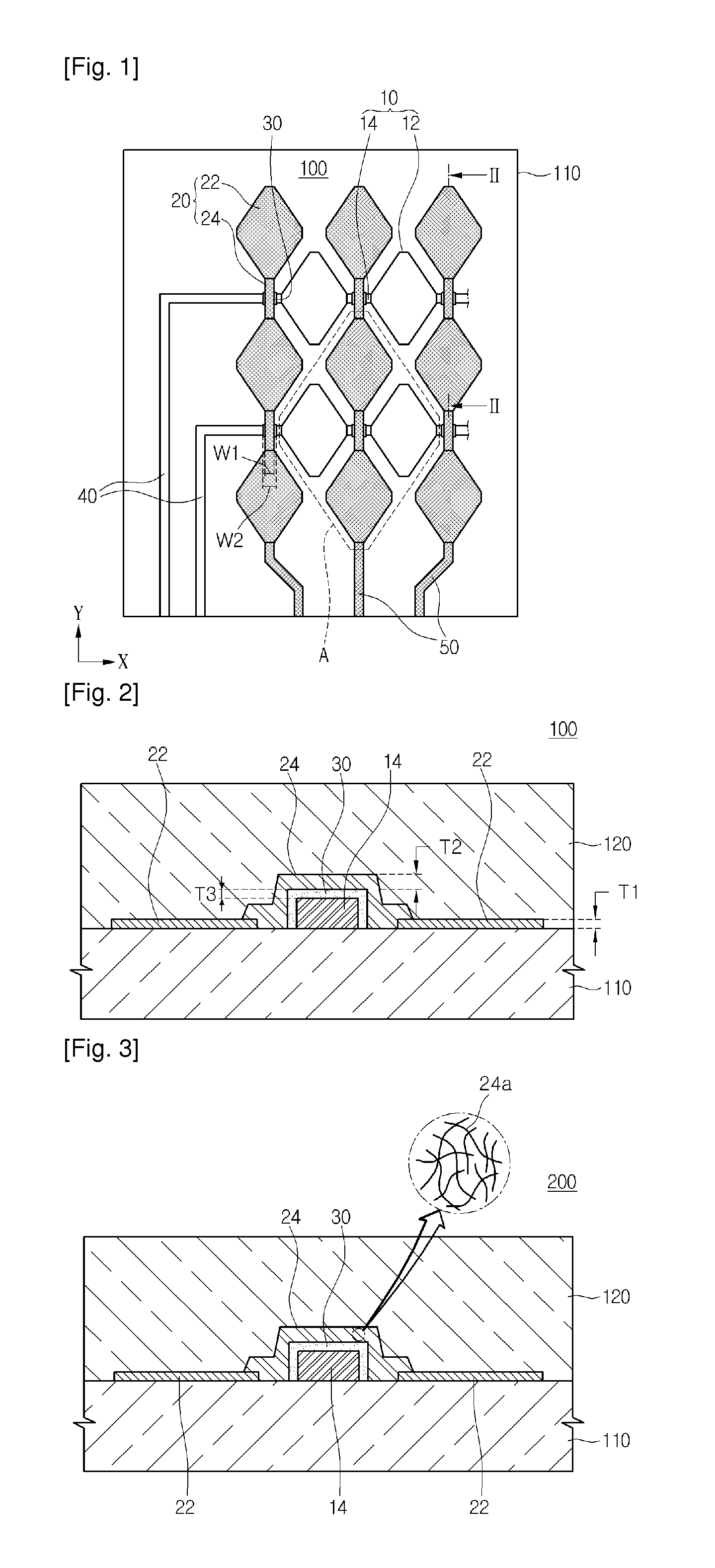
[0045]FIG. 3 is a sectional view of the touch panel according to the

[0046]Referring to FIG. 3, the touch panel 200 according to the second embodiment includes a second connection part 24 having nano wires 24a. The nano wires 24a are connected to each other by a binder (not shown). Since the second connection part 24 includes the nano wires 24a, the second connection part 24 may have the superior optical and electric characteristics. In detail, the transparent degree and the transmission degree of the touch panel can be improved while lowering the resistance.

[0047]However, the embodiment is not limited to the above. For instance, the second connection part 24 may include carbon nano tubes connected to each other by the binder.

third embodiment

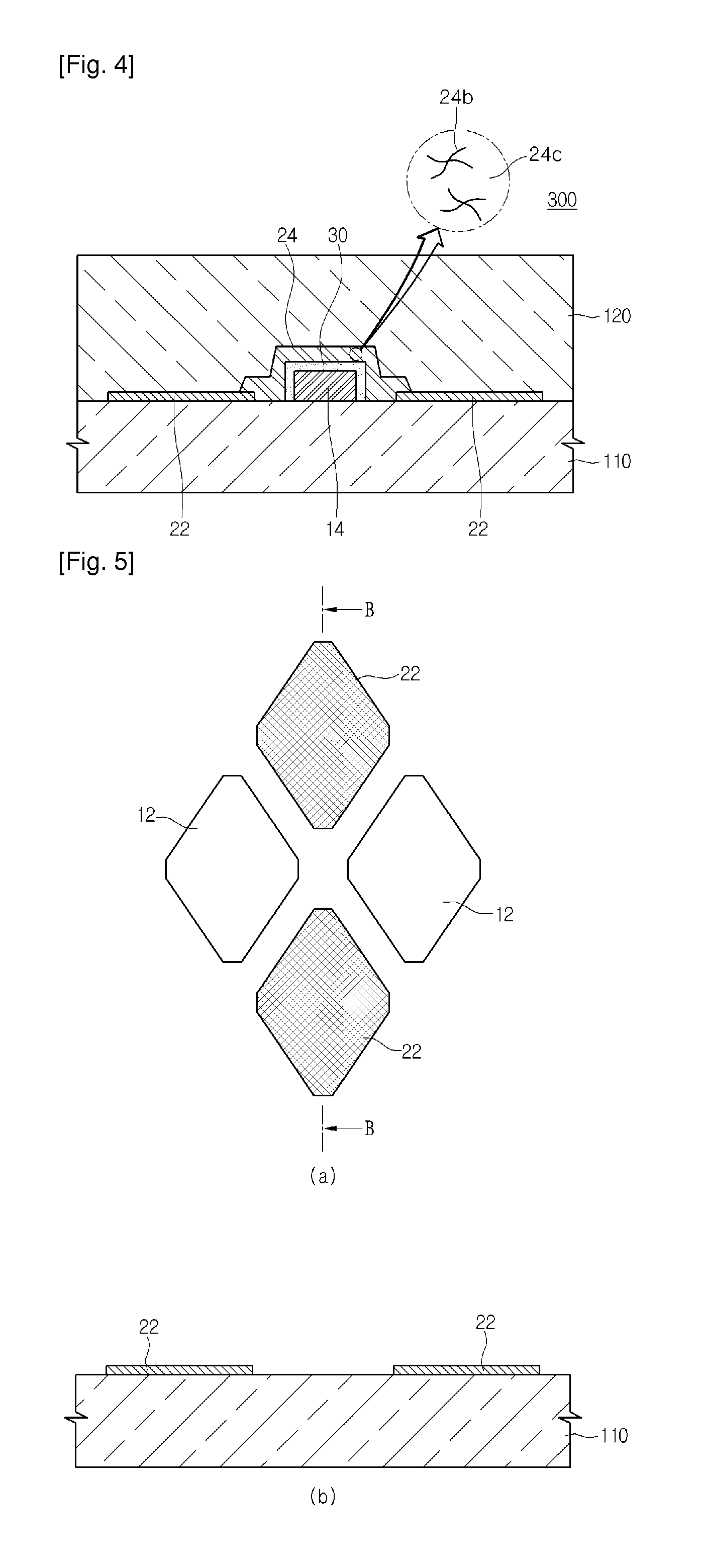
[0048]Hereinafter, the touch panel will be described with reference to FIG. 4.

[0049]FIG. 4 is a sectional view of the touch panel according to the second embodiment.

[0050]Referring to FIG. 4, the touch panel 300 according to the third embodiment includes a second connection part 24. The second connection part 24 may include at least one selected from the group consisting of a carbon nano tube, a nano wire, and a conductive polymer.

[0051]In detail, in the second connection part 24, the nano wires 24b are distributed in the conductive polymer 24c. However, the embodiment is not limited to the above. For instance, carbon nano tubes may be distributed in the conductive polymer instead of the nano wires.

first embodiment

[0052]Hereinafter, the method for manufacturing the touch panel will be described with reference to FIGS. 5 to 8.

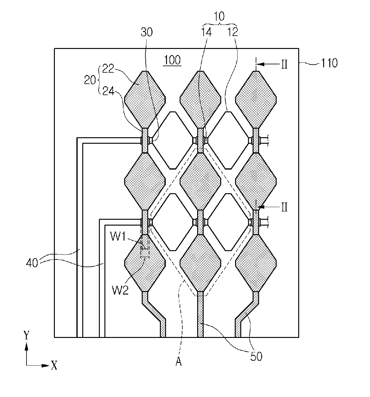
[0053]FIGS. 5 to 8 are plan and sectional views for explaining the method for manufacturing the touch panel according to the first embodiment. In detail, FIGS. 5(a), 6(a), 7(a), and 8(a) are plan views showing the first electrode 10, the second electrode 20 and the insulating layer 30 formed in a region A of FIG. 1, and FIGS. 5(b), 6(b), 7(b), and 8(b) are sectional views taken along line B-B shown in FIGS. 5(a), 6(a), 7(a), and 8(a).

[0054]First, as shown in FIG. 5, a plurality of first sensor parts 12 and a plurality of second sensor parts 22 are formed on the substrate 110 by using the transparent conductive material. The transparent conductive material may include various materials, such as indium tin oxide or indium zinc oxide. The first and second sensor parts 12 and 22 can be formed by depositing the transparent conductive material, for example, through a vacuum de...


PUM

PropertyMeasurementUnit
thicknessaaaaaaaaaa
resistanceaaaaaaaaaa
thickness T3aaaaaaaaaa

Abstract

A touch panel according to the embodiment includes a substrate; a first electrode formed on the substrate in a first direction and including a plurality of sensor parts and connection parts connecting the sensor parts with each other; and a second electrode formed in a second direction crossing the first direction while being insulated from the first electrode and including a plurality of sensor parts and connection parts connecting the sensor parts with each other. The sensor parts and the connection parts include transparent conductive materials, and the connection parts have resistance lower than resistance of the sensor parts in at least one of the first and second electrodes.

Description

TECHNICAL FIELD[0001]The disclosure relates to a touch panel and a method for manufacturing the same.BACKGROUND ART[0002]Recently, touch panels are employed in various electronic appliances to allow a user to input data by touching an image displayed on a display device using an input device, such as a finger or a stylus.[0003]Such touch panels are mainly classified into resistive touch panels and capacitive touch panels. According to the resistive touch panel, an electrode is shorted as pressure is applied thereto from an input device so that a position is detected. According to the capacitive touch panel, capacitance between electrodes is varied as a finger touches the touch panel and a position is detected based on the capacitance variation.[0004]The performance of the resistive touch panel may be degraded if the resistive touch panel is repeatedly used for a long time, and scratch may be generated. For this reason, the capacitive touch panel has been spotlighted due to the super...

Claims


Application Information

Patent Timeline
Patent Type & Authority Applications(United States)
IPC IPC(8): G06F3/044
CPCG06F3/044G06F2203/04111G06F3/0443G06F3/0446
Inventor LEE, DONG YOULLEE, YONG JINYOU, YOUNG SUNCHAI, KYOUNG HOONNOH, YOUNG JIN
Owner LG INNOTEK CO LTD
Why Eureka
Try Eureka