

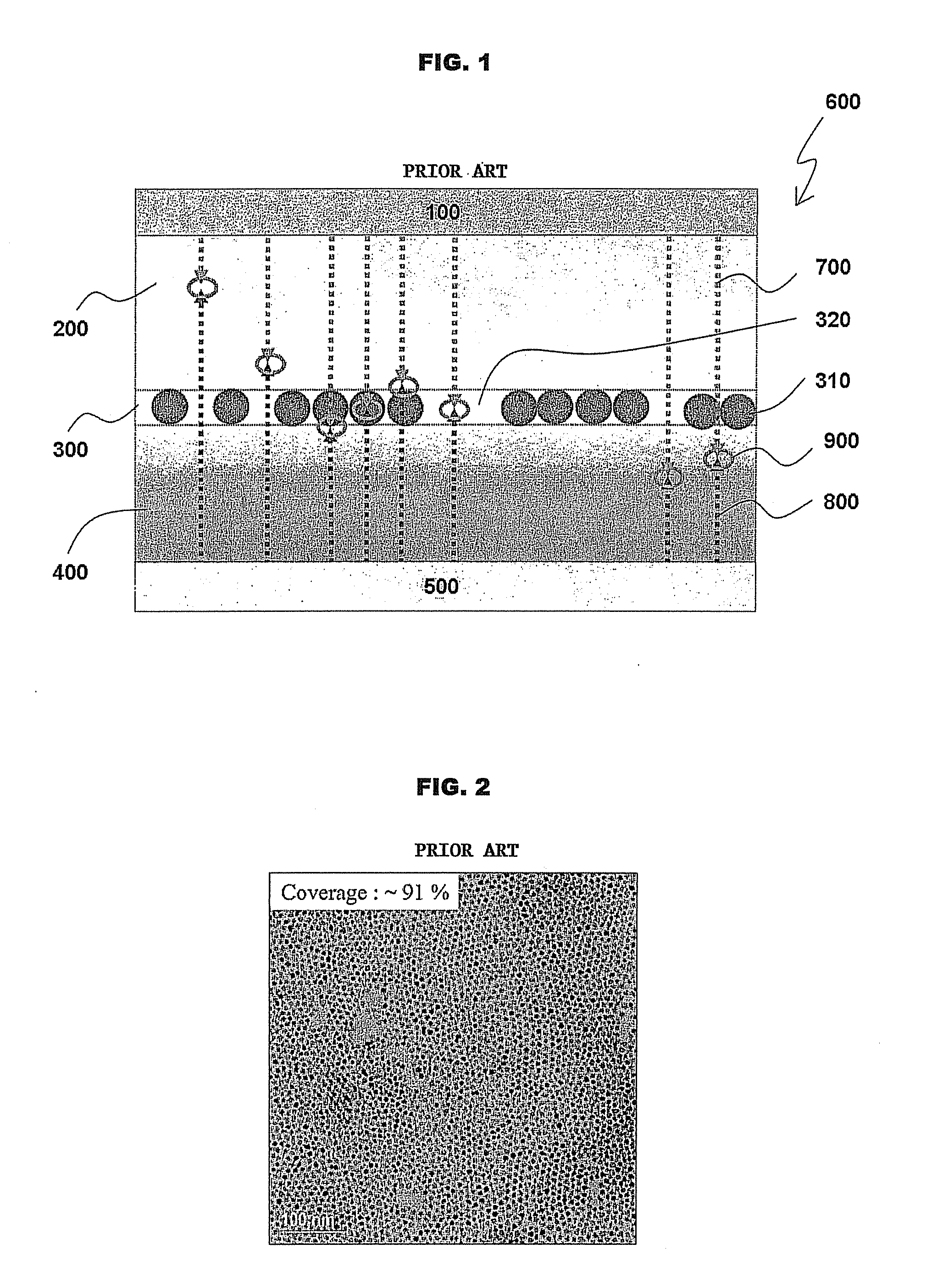
Light-emitting device comprising semiconductor nanocrystal layer free of voids and method for producing the same
a technology of semiconductor nanocrystals and light-emitting devices, which is applied in the direction of semiconductor devices, material nanotechnology, electrical devices, etc., can solve the problems of reducing the luminescence efficiency of light-emitting devices, current leakage, and inability to achieve light-emitting, and achieve excellent electrical stability and high efficiency
- Summary
- Abstract
- Description
- Claims
- Application Information
AI Technical Summary
Benefits of technology
Problems solved by technology
Method used
Image

Examples
example 1
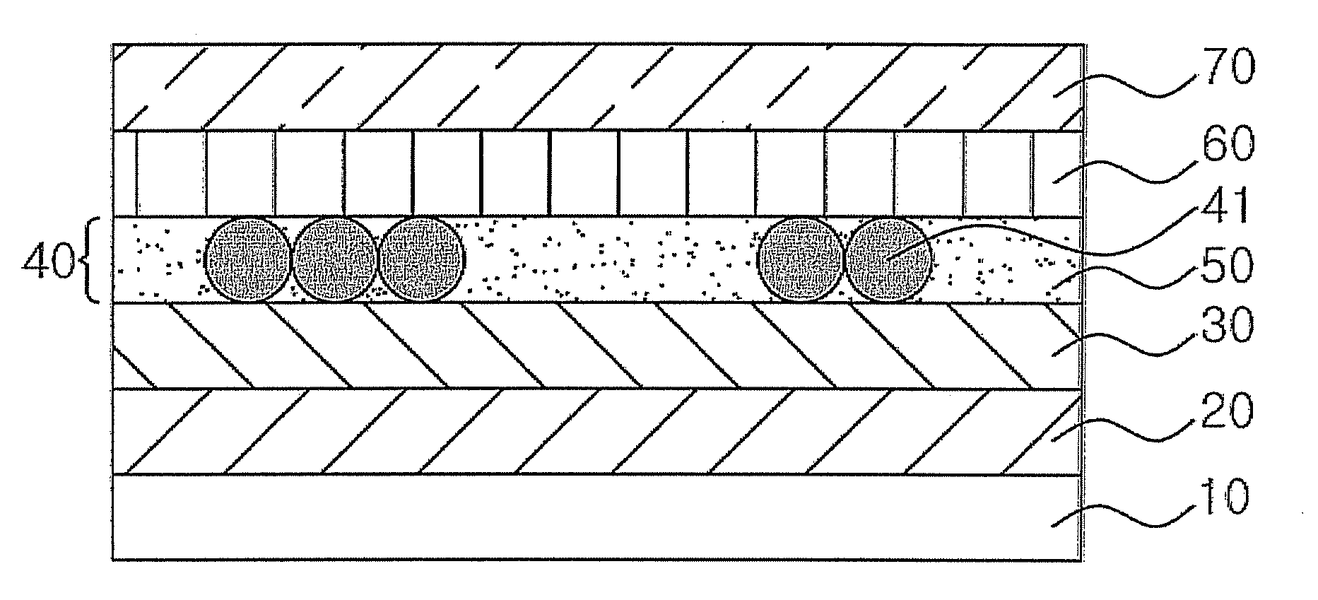
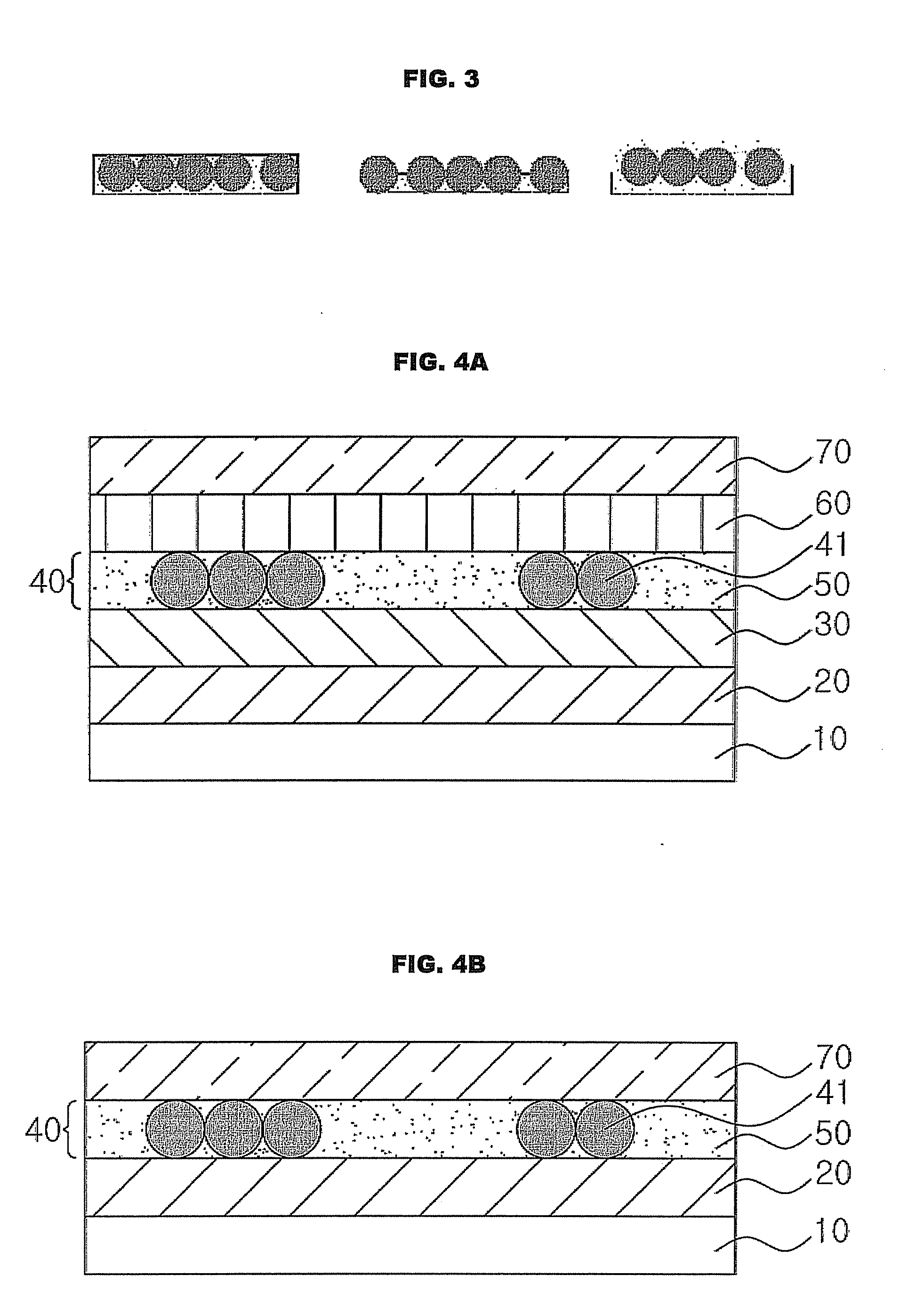
Fabrication of Light-Emitting Device Including Nanocrystal Layer Whose Voids are Filled with Filling Material
[0082]A TiO2 precursor (DuPont Tyzor, BTP, 2.5 wt % in butanol) was spin-coated on a patterned ITO substrate at 2,000 rpm under a nitrogen atmosphere for 30 seconds, dried under a nitrogen atmosphere for about 5 minutes, and annealed at 150° C. for 15 minutes to form an amorphous TiO2 thin film having a thickness of about 20 nm.
[0083]A solution (0.3 wt %) of red-emitting (642 nm) CdSe / ZnS core / shell structured quantum dots QD (diameter: about 6 nm, Evident Tech. Inc.) in chloroform was spin-coated on the TiO2 thin film at 2,000 rpm for 30 seconds, and dried at 50° C. for 5 minutes to arrange the quantum dots QD in a single layer. 3-(4-biphenyl)-4-phenyl-5-tert-butylphenyl-1,2,4-triazole (TAZ) was filled on the quantum dots QD to form a semiconductor nanocrystal layer. N,N′-di(naphthalen-1-yl)-N—N′-diphenyl-benzidine (a-NPB) was filled to a thickness of about 40 nm on the semi...
experimental example 1
Comparison of Stability of Light-Emitting Devices
[0085]To evaluate the stability of the light-emitting devices produced in Example 1 and Comparative Example 1, the luminescence spectra, luminescence intensity per unit area, and changes in the amount of current flowing through the devices were measured at ambient temperature and pressure with increasing voltage applied to the devices.
[0086]FIGS. 7A and 7B are graphs showing luminescence spectra of the light-emitting devices produced in Example 1 and Comparative Example 1, respectively, with increasing voltage applied to the devices.
[0087]FIGS. 8A and 8B are graphs showing changes in luminescence intensity per unit area of the light-emitting devices produced in Example 1 and Comparative Example 1, respectively, with increasing voltage applied to the devices.
[0088]These graphs show that the intensity of light emitted from the light-emitting devices increases with increasing voltage applied to the devices.
[0089]FIGS. 9A and 9B are graph...
experimental example 2
Comparison of Luminescence Efficiency of Light-Emitting Devices
[0091]To measure the luminescence efficiency of the light-emitting devices produced in Example 1 and Comparative Example 1, the luminescence intensity per unit current of the devices was measured at ambient temperature and pressure with increasing voltage applied to the devices.
[0092]FIGS. 10A and 10B are graphs showing changes in luminescence efficiency per unit current of the light-emitting devices produced in Example 1 and Comparative Example 1, respectively, with increasing voltage applied to the devices.
[0093]The graph of FIG. 10B shows that the luminescence efficiency per unit current of the light-emitting device produced in Comparative Example 1 gradually increases until it reaches a maximum at 13V and thereafter begins to rapidly decrease. In contrast, the graph of FIG. 10A shows that the luminescence efficiency of the light-emitting device produced in Example 1 is maintained at a high level from the beginning of...
PUM
 Abstract
Description
Claims
Application Information