Integrated circuit packaging body and preparation method thereof

A technology for integrated circuits and packages, which is applied in the field of integrated circuit packages and their preparation, can solve problems such as open solder joints and failure of integrated circuit packages, and achieve the goal of improving yield, ensuring high consistency, and reducing the probability of open circuits Effect

CN111063667AActive Publication Date: 2020-04-24NANTONG FUJITSU MICROELECTRONICS
4 Cites 0 Cited by

Patent Information

Authority / Receiving Office
CN · China
Patent Type
Applications(China)
Current Assignee / Owner
Publication Date
2020-04-24

Smart Images

  • Figure 1
    Figure 1
  • Figure 2
    Figure 2
  • Figure 3
    Figure 3
Patent Text Reader

Abstract

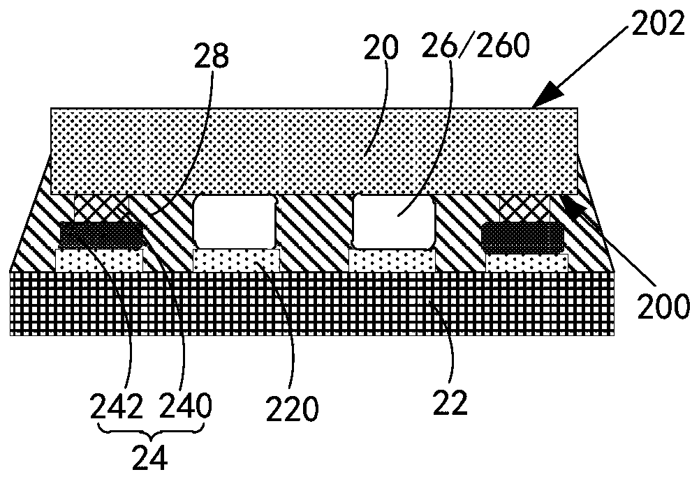
The invention provides an integrated circuit packaging body and a preparation method thereof. The packaging body comprises a chip which comprises a functional surface and a non-functional surface which are oppositely arranged, and the functional surface is provided with a plurality of first bonding pads which are arranged at intervals. The packaging body further comprises a substrate, wherein thesubstrate and the chip are oppositely arranged at intervals. A second bonding pad is arranged at the position, corresponding to the first bonding pad, of the substrate. The packaging body further comprises a number of first welding bodies. Each first welding body comprises a conductive supporting piece and a first welding flux layer at least located at the end of one side of the conductive supporting piece, and the first welding bodies are electrically connected between part of the first bonding pads and the corresponding second bonding pads. The packaging body further comprises a number of second welding bodies which comprise second welding flux layers, and the second welding bodies are electrically connected between the remaining first bonding pads and the corresponding second bonding pads. The melting point of the conductive supporting pieces is greater than the melting points of the first welding flux layer and the second welding flux layer. According to the invention, the probability that the chip inclines relative to the substrate during backflow can be reduced.
Need to check novelty before this filing date? Find Prior Art

Description

technical field

[0001] The present application relates to the field of packaging technology, in particular to an integrated circuit package and a preparation method thereof. Background technique

[0002] Among integrated circuit packages, ball array packaging is a relatively common product packaging method. The packaging method specifically includes: using a ball planting machine to form solder balls on the first pad of the chip, and then using surface mount technology to mount and reflow solder the chip and the substrate.

[0003] The inventors of the present application have found in the long-term research process that during the reflow soldering process of the above-mentioned integrated circuit package, due to the warpage of the substrate or the tilt of the chip during mounting, the solder balls on the chip may not match the solder balls at the corresponding positions. The second pad on the substrate is connected, thereby causing an open circuit of the solder joint, so t...

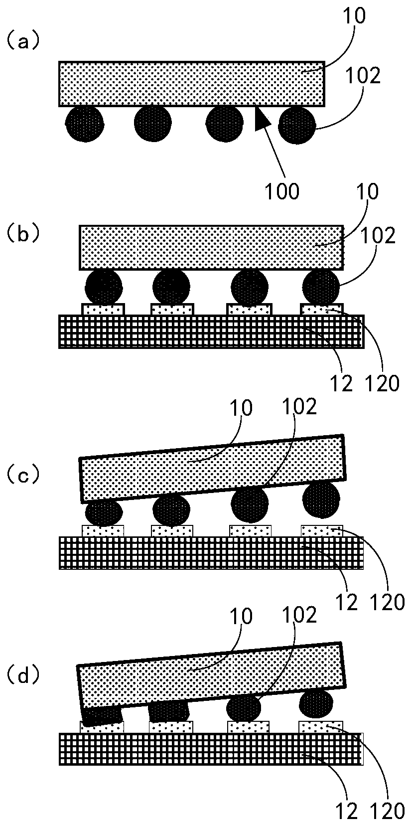
Examples

Embodiment Construction

[0027] The following will clearly and completely describe the technical solutions in the embodiments of the present application with reference to the drawings in the embodiments of the present application. Obviously, the described embodiments are only some of the embodiments of the present application, not all of them. Based on the embodiments in this application, all other embodiments obtained by persons of ordinary skill in the art without making creative efforts belong to the scope of protection of this application.

[0028] see figure 1 , figure 1 It is a structural schematic diagram of an embodiment corresponding to the manufacturing method of the integrated circuit package in the prior art. Such as figure 1 As shown in a, balls are normally planted on the first pad (not shown) on the functional surface 100 of the chip 10, and all solder balls 102 can be planted at one time; figure 1 As shown in b, the chip 10 is flip-chip mounted on the substrate 12, and the solder ba...