
Magnetic jig and multilayer FPC welding method
A welding method and magnetic technology, applied in the manufacture of printed circuits, electrical components, printed circuits, etc., can solve the problems of low utilization rate of circuit boards, low welding accuracy, high labor costs, etc., to improve poor welding, avoid false welding, The effect of low coefficient of friction
- Summary
- Abstract
- Description
- Claims
- Application Information
AI Technical Summary
Problems solved by technology
Method used
Image

Examples
Embodiment Construction
[0032] In order to make the purpose, technical solutions and advantages of the present invention more clear, the present invention will be further described in detail below in conjunction with the accompanying drawings and implementation examples. It should be understood that the specific embodiments described here are only used to explain the present invention, not to limit the present invention.
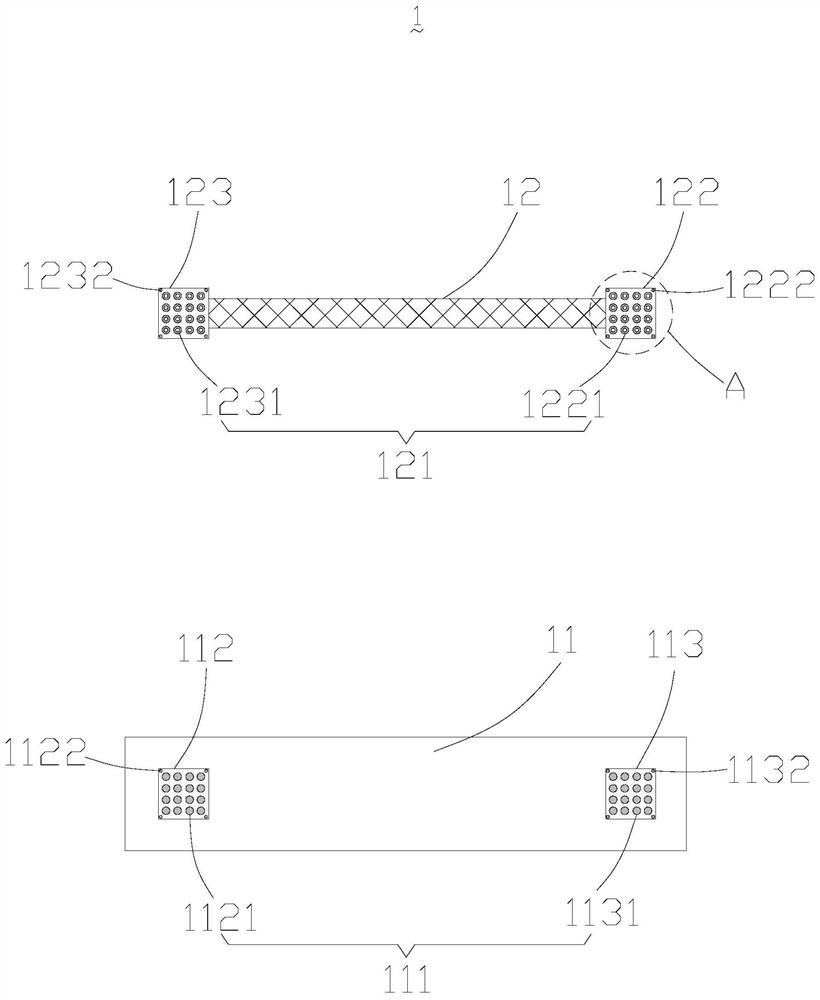
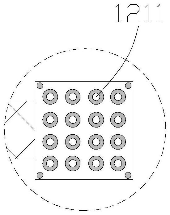
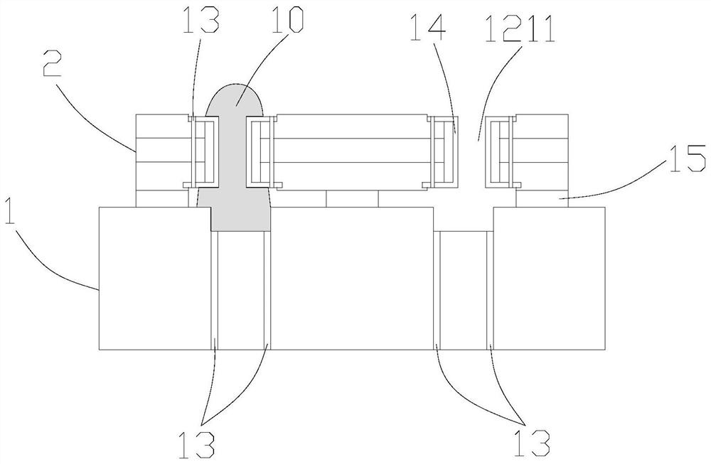
[0033] see figure 1 and figure 2, the first embodiment of the present invention provides a multilayer interconnection electronic circuit board 1, the multilayer interconnection electronic circuit board 1 includes a main board 11 and one or more jumper boards 12, and the jumper boards 12 are far away from the main board One side of 11 is provided with a jumper line (not shown in the figure), and the side of the jumper board 12 close to the main board 11 is provided with a plurality of docking pads 121, and the butt pads 121 are provided with via holes 1211, The connecting pad 121...
PUM
 Abstract
Description
Claims
Application Information