Display panel and display device

A display panel and display area technology, which is applied in the direction of semiconductor devices, electrical components, circuits, etc., can solve the problems of OLED device luminous brightness and color deviation, and affect the display effect of the display panel, so as to simplify the structure, improve the display effect and reduce the cost Effect

Active Publication Date: 2021-07-02
XIAMEN TIANMA MICRO ELECTRONICS
View PDF8 Cites 7 Cited by
  • Summary
  • Abstract
  • Description
  • Claims
  • Application Information

AI Technical Summary

Problems solved by technology

However, when an OLED display panel is applied to a display device, the driving transistor in the display panel is affected by an external electric field, and the generated driving current deviates from the theoretically generated driving current, which makes the luminous brightness and color of the OLED device deviate. Thus affecting the display effect of the display panel

Method used


Image

  • Display panel and display device
  • Display panel and display device
  • Display panel and display device

Examples


Embodiment Construction

[0027] The present invention is further detailed in conjunction with the accompanying drawings and examples. It will be appreciated that the specific embodiments described herein are merely illustrative of the invention and are not limited thereto. It will also be noted that in order to facilitate the description, only the parts associated with the present invention are shown in the drawings rather than all structures.

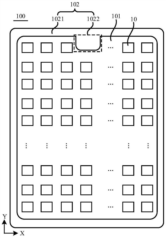
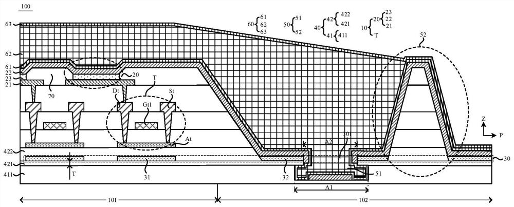
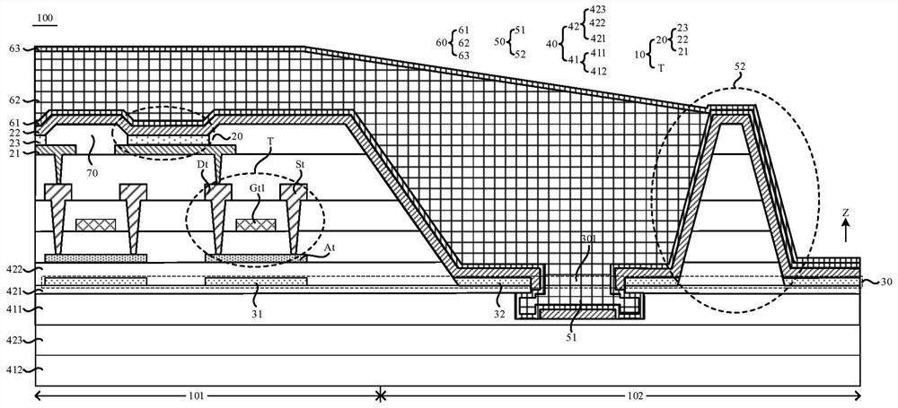
[0028] As described in the background, since the OLED device is a current type driving element such that the OLED display panel needs to be provided for driving the OLED device to perform light emission, the drive transistor of the pixel circuit can generate corresponding according to the data signals thereof. The current to the OLED device such that the OLED device emits light according to the size of the drive current. Therefore, when the drive transistor is interference from the external electric field (e.g., an electric field generated by impurities and / or d...


PUM


Abstract

The embodiment of the invention discloses a display panel and a display device. The display panel comprises a display area and a non-display area; a substrate which comprises at least one organic layer and at least one inorganic layer, wherein the organic layer and the inorganic layer are arranged in a stacked mode; a plurality of pixel circuits, wherein each pixel circuit comprises a driving transistor; a driving transistor which comprises a first active layer; a semiconductor layer which comprises a shielding structure and an etching blocking structure, wherein the shielding structure is located in the display area, the vertical projection of the shielding structure on the film layer where the first active layers are located is overlapped with the first active layers, the etching blocking structure is located in the non-display area, and the etching blocking structure comprises at least one opening; and a blocking unit located in the non-display area, wherein the blocking unit comprises at least one groove structure and the groove structure penetrates through the first inorganic layer from the opening in the direction perpendicular to the plane where the first organic layer is located and extends into the first organic layer. According to the embodiment of the invention, the process cost of the display panel can be reduced, and the display effect of the display panel is improved.

Description

Technical field [0001] Embodiments of the present invention relate to the field of display, and more particularly to a display panel and a display device. Background technique [0002] Organic Light Emitting Diode, OLED Monitor has the advantages of self-illuminating, low power, wide viewing angle, and fast response speed, and is more considered to have a wide range of application prospects in various fields. [0003] A display device including an OLED display is typically composed of an OLED display panel, a system motherboard, and a housing, and the system motherboard can provide a corresponding display signal to the OLED display panel to control the OLED display panel to display the corresponding screen. The OLED display panel is typically provided with an OLED device for displaying a light-emitting device and a driving transistor for driving the OLED device to produce a respective drive current to drive the OLED device. However, because the OLED display panel is applied to th...

Claims


Application Information

Patent Timeline
Patent Type & Authority Applications(China)
IPC IPC(8): H01L27/32H01L51/52
CPCH10K59/126H10K50/844
Inventor 何水陈秋男
Owner XIAMEN TIANMA MICRO ELECTRONICS
Why Eureka
Try Eureka