
Semiconductor device and manufacturing method thereof
A manufacturing method and semiconductor technology, which are used in semiconductor/solid-state device manufacturing, semiconductor devices, semiconductor/solid-state device components, etc., can solve problems such as unsatisfactory protection effect of sealing rings, and prevent cracks from spreading toward the integrated circuit area. Improves shielding, preventing moisture and ions from entering the integrated circuit area
- Summary
- Abstract
- Description
- Claims
- Application Information
AI Technical Summary
Problems solved by technology
Method used
Image

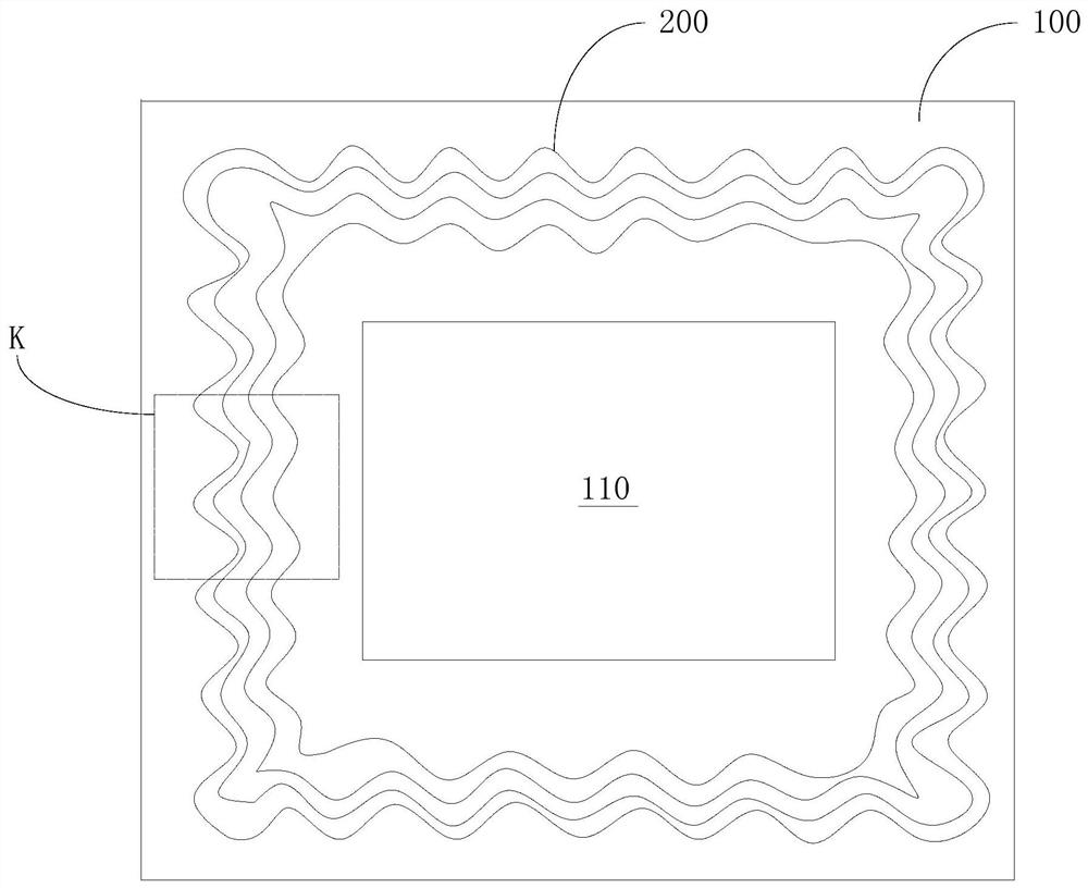
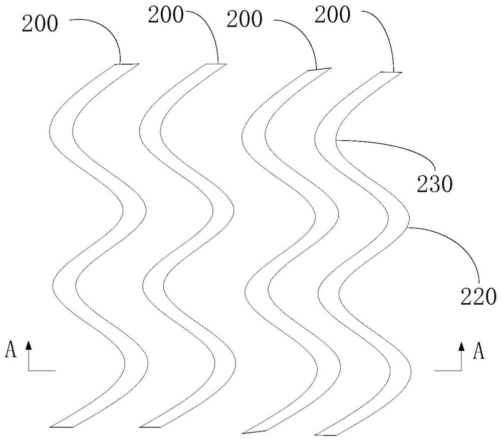
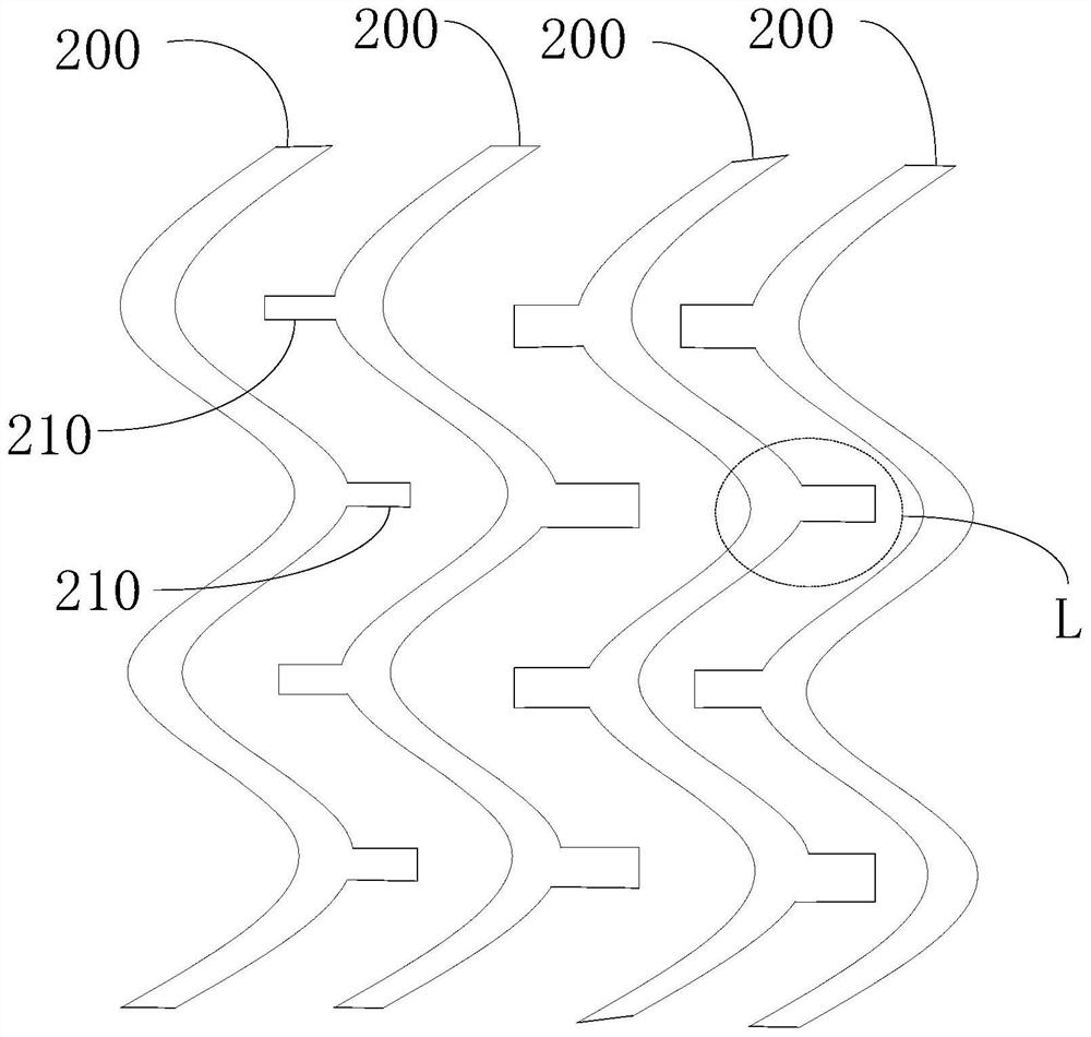
Examples
Embodiment Construction
[0051] Example embodiments will now be described more fully with reference to the accompanying drawings. Example embodiments may, however, be embodied in many forms and should not be construed as limited to the embodiments set forth herein; rather, these embodiments are provided so that this disclosure will be thorough and complete, and will fully convey the concept of example embodiments to those skilled in the art. The same reference numerals in the drawings denote the same or similar structures, and thus their detailed descriptions will be omitted.
[0052] Semiconductor devices are often provided with a sealing ring extending around the periphery of an integrated circuit area of the semiconductor device. A seal ring is usually a continuous ring of one or more metal layers. In one or more example embodiments, the seal ring may have one or more functions of providing protection from external moisture from entering integrated circuit components formed in the semiconductor...
PUM
 Abstract
Description
Claims
Application Information