Thin film transistor array panel and liquid crystal display including the panel

A technology of thin film transistors and array panels, applied in the field of liquid crystal displays, can solve problems such as the reduction of aperture ratio

CN1650223AInactive Publication Date: 2005-08-03SAMSUNG DISPLAY CO LTD
0 Cites 10 Cited by

Patent Information

Authority / Receiving Office
CN · China
Current Assignee / Owner
Publication Date
2005-08-03
Estimated Expiration
Not applicable · inactive patent

Smart Images

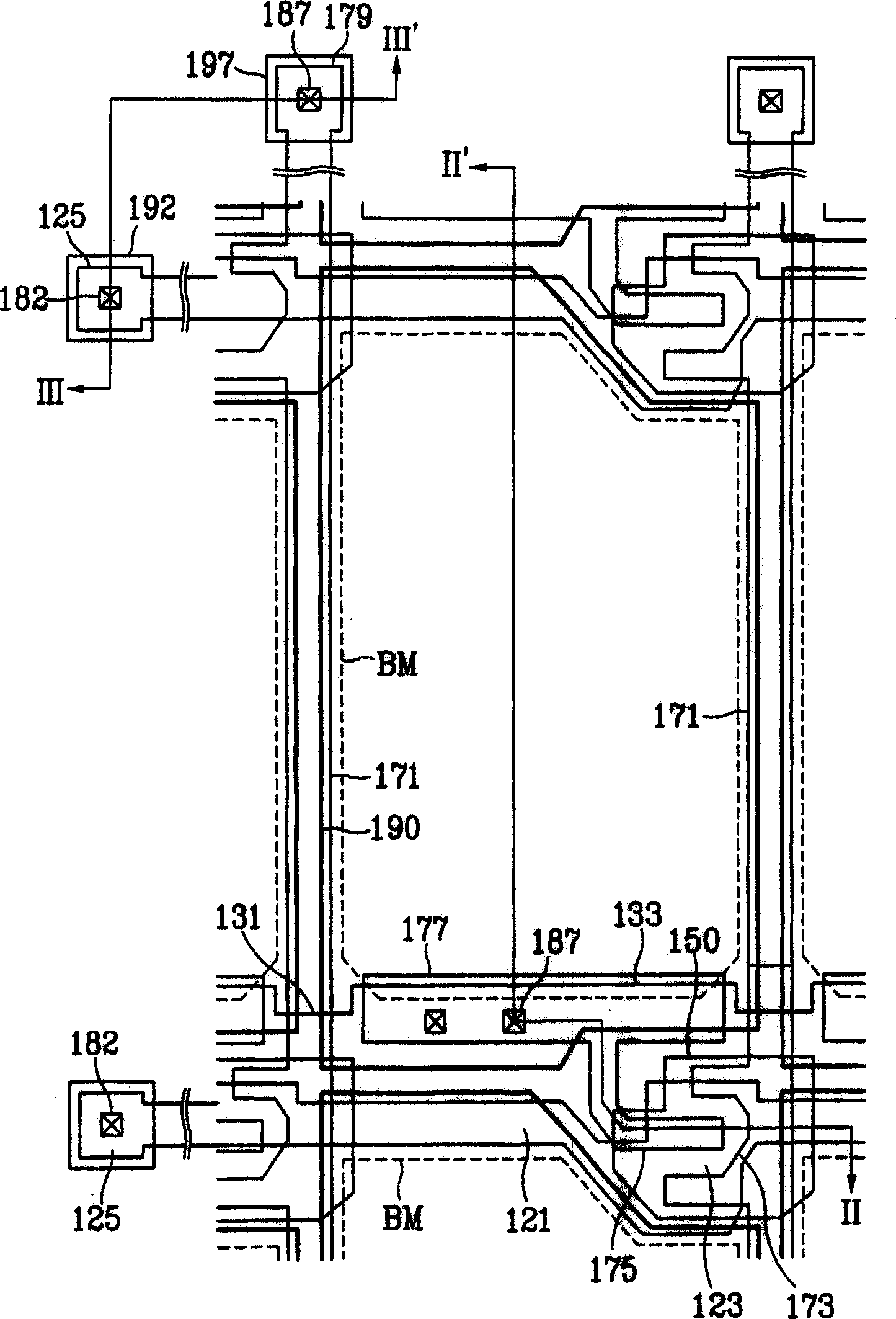
  • Figure 1
    Figure 1
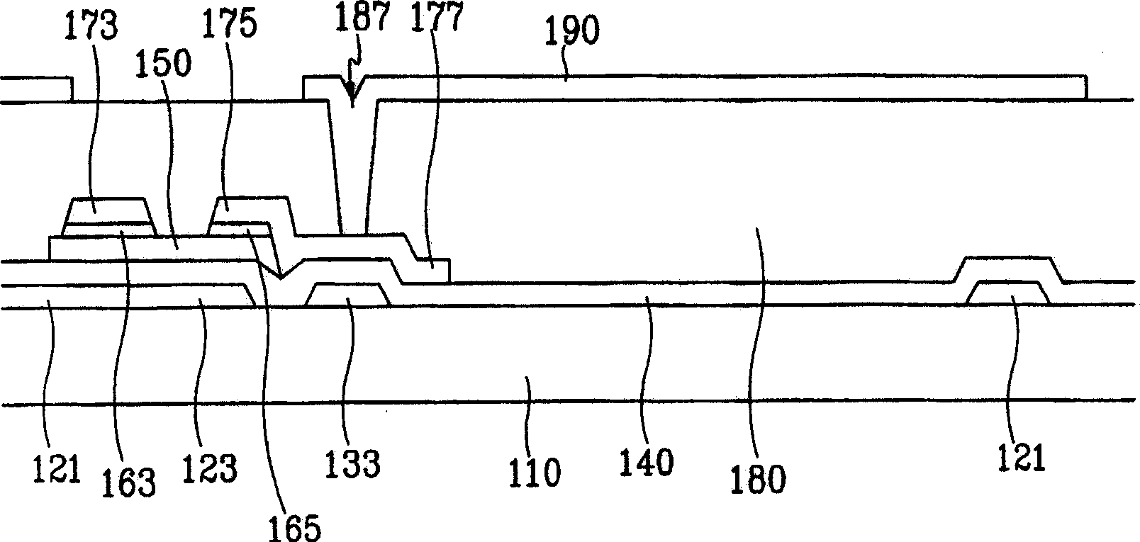
  • Figure 2
    Figure 2
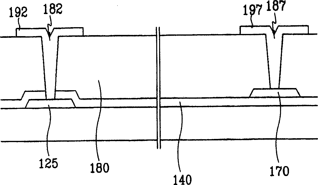
  • Figure 3
    Figure 3
Patent Text Reader

Abstract

A gate wire including a gate line extending in a transverse direction and a gate electrode connected to the gate line is form on an insulating substrate. A storage capacitor wire including a storage capacitor electrode line extending in the transverse direction and a storage electrode connected to the storage capacitor electrode line and located at the edges of a pixel area is formed. A semiconductor layer is formed on a gate insulating film covering the gate wire and the storage capacitor wire. A data wire is formed on the gate insulating film or the semiconductor layer and includes a data line intersecting the gate line to define the pixel area, a source electrode connected to the data line and located on the semiconductor layer, a drain electrode formed on the semiconductor layer and located opposite the source electrode with respect to the gate electrode, and a first storage capacitor conductor overlapping the storage capacitor electrode via the gate insulating film to form a storage capacitor. A pixel electrode electrically connected to the drain electrode and the first storage capacitor conductor is formed on the protective layer covering the data wire.
Need to check novelty before this filing date? Find Prior Art

Description

technical field

[0001] The present invention relates to a thin film transistor array panel and a liquid crystal display including the thin film transistor array panel, more specifically, relates to a thin film transistor array panel including a storage electrode overlapping with a pixel electrode to form a storage capacitor and a thin film transistor array panel Panel LCD display. Background technique

[0002] A liquid crystal display ("LCD") is the most widely used type of flat panel display. A liquid crystal display includes two panels having a plurality of electrodes generating an electric field, a liquid crystal layer interposed therebetween, and two polarizing plates respectively polarizable and attached to outer surfaces of the two panels. The liquid crystal display controls the transmittance of light passing through the liquid crystal layer by rearranging liquid crystal molecules of the liquid crystal layer using voltage applied to electrodes. Liquid crystal display...

Examples

Embodiment Construction

[0015] In order to enable those skilled in the art to practice the present invention, preferred embodiments of the present invention will be described in detail below with reference to the accompanying drawings. However, the present invention can be embodied in various forms, and it is not limited to the embodiments described here.

[0016] In the drawings, the thicknesses and regions of layers are exaggerated for clarity. Throughout the specification, the same symbols are attached to the same elements. It should be understood that when an element such as a layer, film, region, or substrate is referred to as being "on" another part, it means that it is located directly on the other element. , or there may be other components in between. In contrast, when an element is referred to as being "directly" on other elements, it means that there are no intervening elements.

[0017] Hereinafter, a thin film transistor array panel and a liquid crystal display including the thin film ...