Multilayer type electrophotographic photoconductor and image forming apparatus

a photoconductor and photoconductor technology, applied in the direction of electrographic process, instruments, corona discharge, etc., can solve the problems of insufficient charge transporting ability, image characteristic deterioration due to the charge accumulation inside the layer, and easy lowering of charge transporting ability in the charge generating layer, etc., to achieve low generation and high image quality

Active Publication Date: 2007-12-06
KYOCERA DOCUMENT SOLUTIONS INC
View PDF5 Cites 25 Cited by
  • Summary
  • Abstract
  • Description
  • Claims
  • Application Information

AI Technical Summary

Benefits of technology

[0031]According to the image forming apparatus, the light absorption degree of a predetermined wavelength in the photoconductive layer can be limited so that a high image quality image can be provided over a long term with little generation of the exposure memory and the photo memory.

Problems solved by technology

However, since the multilayer type organic photoconductor contains the charge generating agent and the charge transporting agent in different layers, the charge transporting ability in the charge generating layer can easily be lowered so that a problem of the image characteristic deterioration due to the charge accumulation inside the layer is involved.
In particular, problems of generation of the so-called exposure memory of transferring the charge generated in the previous rounds and accumulated inside the charge generating layer to an image in the following rounds, or the so-called photo memory of the influence to the evenness of the initial charge caused by the charge generated by the external beam accumulated inside the charge generating layer have been observed.
In particular, depending on the kind of the charge generating agent or the charge transporting agent, the charge transporting ability may not be sufficiently obtained, or on the contrary, due to the excessive sensitivity to the exposure light source, the exposure memory may be generated.

Method used


Image

  • Multilayer type electrophotographic photoconductor and image forming apparatus
  • Multilayer type electrophotographic photoconductor and image forming apparatus
  • Multilayer type electrophotographic photoconductor and image forming apparatus

Examples


first embodiment

[0044]A first embodiment of the present invention is a multilayer type electrophotographic photoconductor comprising a charge generating layer containing at least a charge generating agent on a base member directly or via an intermediate layer, and a charge transporting layer containing at least a charge transporting agent and a binder resin formed successively, wherein the light absorption degree at a 680 nm wavelength light beam in the photoconductive layer of the multilayer type electrophotographic photoconductor is of a value of 0.8 or less, and the light absorption degree at a 450 nm wavelength light beam is of a value of 1.0 or more. Hereafter, the multilayer type electrophotographic photoconductor of the first embodiment will be explained specifically.

1. Basic Configuration

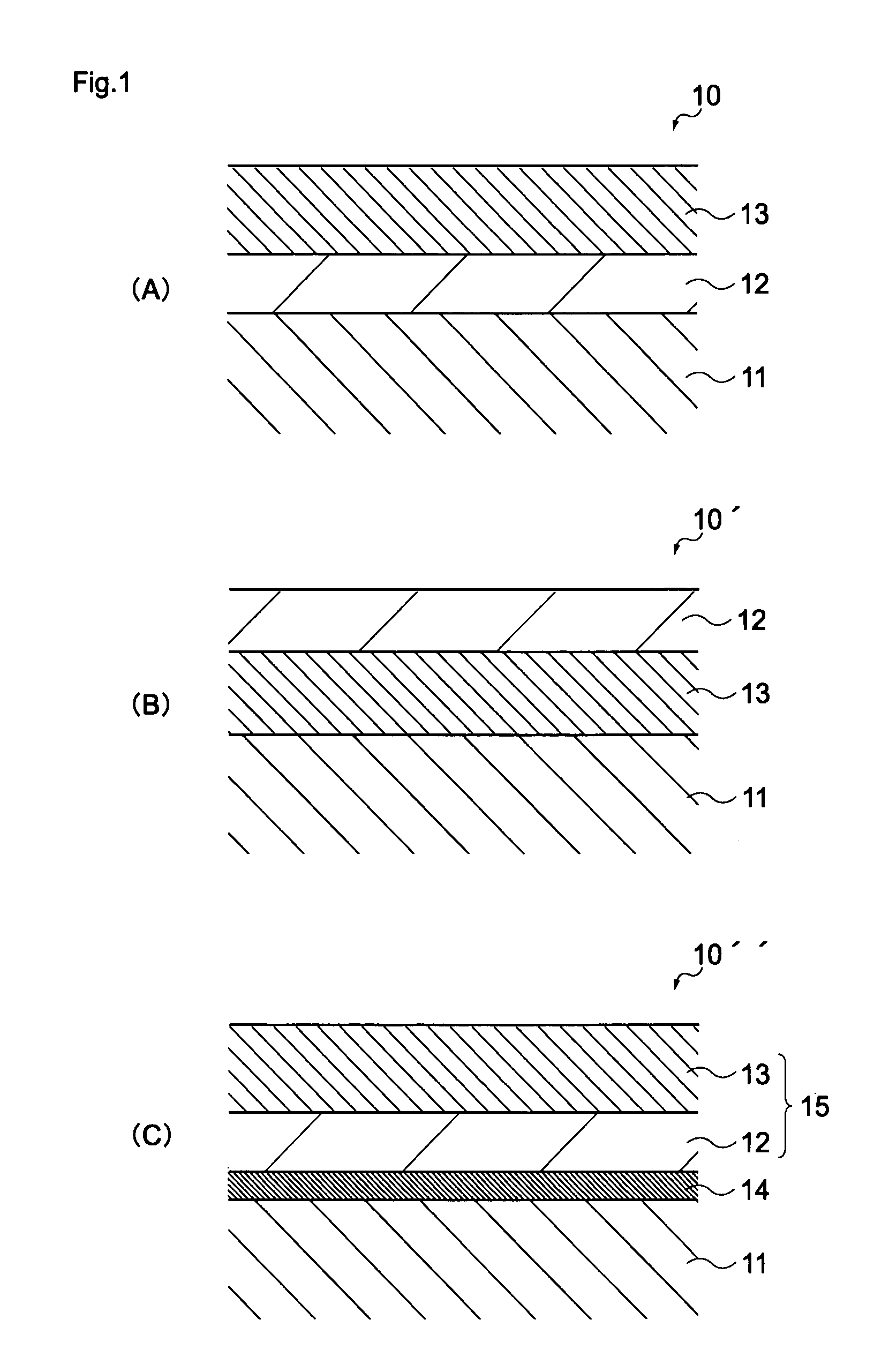
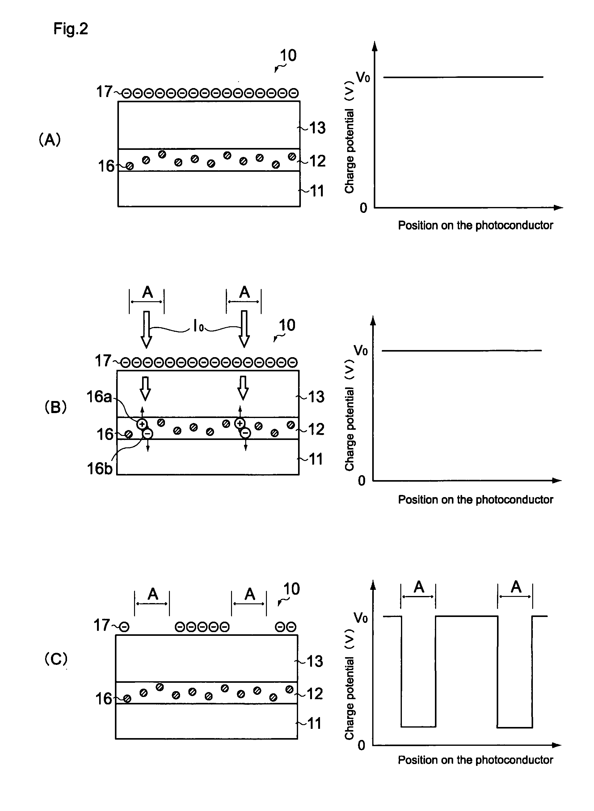
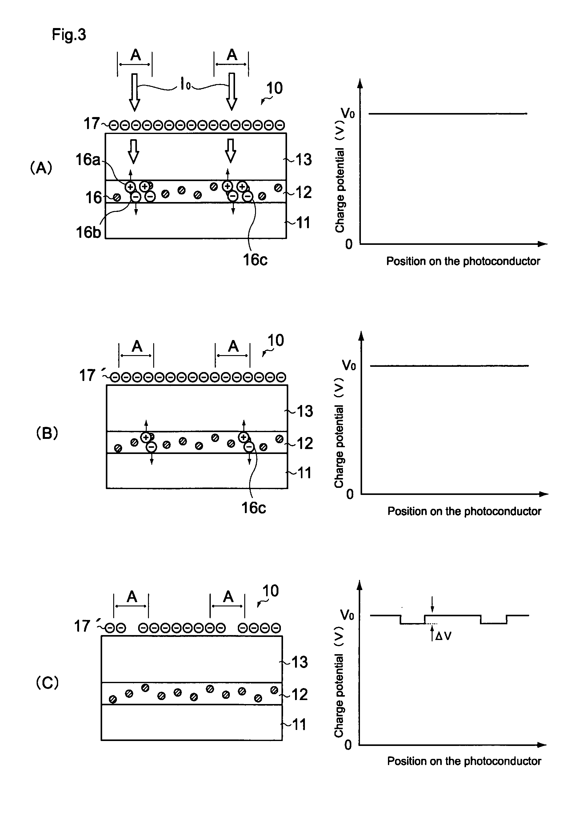
[0045]As shown in FIG. 1A, a multilayer type electrophotographic photoconductor 10 of the present invention has a multilayer structure comprising a charge generating layer 12 containing a charge generating ...

second embodiment

[0178]A second embodiment is an image forming apparatus comprising a multilayer type electrophotographic photoconductor having a charge generating layer containing at least a charge generating agent on a base member directly or via an intermediate layer, and a charge transporting layer containing at least a charge transporting agent and a binder resin formed successively, wherein a charging means, an exposure means, a developing means and a transfer means are provided around the multilayer type electrophotographic photoconductor, the light absorption degree at a 680 nm wavelength light beam in the photoconductive layer of the multilayer type electrophotographic photoconductor is of a value of 0.8 or less, and the light absorption degree at a 450 nm wavelength light beam is of a value of 1.0 or more.

[0179]Hereafter, the second embodiment will be explained mainly on the points different from those of the first embodiment while omitting the content already described in the first embodi...

example 1

1. Production of the Multilayer Type Electrophotographic Photoconductor

(1) Production of the Intermediate Layer

[0192]An intermediate layer (lower layer) coating solution was prepared by placing in a container 2 parts by weight of a titanium oxide (produced by TEIKA Corp., SMT-02, numeral average primary particle size: 10 nm) with the surface treatment with methyl hydrogen polysiloxane while wet dispersion after the surface treatment with alumina and silica, 1 part by weight of a four element copolymerized polyamide resin (produced by Toray Corp., AMIRAN CM8000), 10 parts by weight of methanol, and 2 parts by weight of butanol, and dispersing for 5 hours using a bead mill (medium: a 0.5 mm diameter zirconia ball).

[0193]Then, after filtrating the obtained intermediate layer coating solution with a 5 μm filter, it was coated onto an aluminum base member having a 30 mm diameter and a 238.5 mm length by using a dip coating method with a 5 mm / sec drawing rate.

[0194]Finally, by applying a ...


PUM

PropertyMeasurementUnit
wavelengthaaaaaaaaaa
wavelength rangeaaaaaaaaaa
2θ±0aaaaaaaaaa

Abstract

The present invention is to provide a multilayer type electrophotographic photoconductor capable of stably obtaining a high image quality image over a long term by restraining the exposure memory and the photo memory, and an image forming apparatus comprising such a multilayer type electrophotographic photoconductor. A multilayer type electrophotographic photoconductor comprising a charge generating layer containing at least a charge generating agent on a base member directly or via an intermediate layer, and a charge transporting layer containing at least a charge transporting agent and a binder resin formed successively, wherein the light absorption degree at a 680 nm wavelength light beam in the photoconductive layer of the multilayer type electrophotographic photoconductor is of a value of 0.8 or less, and the light absorption degree at a 450 nm wavelength light beam is of a value of 1.0 or more, and an image forming apparatus comprising such a multilayer type electrophotographic photoconductor are provided.

Description

BACKGROUND OF THE INVENTION[0001]1. Field of the Invention[0002]The present invention relates to a multilayer type electrophotographic photoconductor and an image forming apparatus. In particular, it relates to a multilayer type electrophotographic photoconductor capable of restraining generation of the exposure memory and the photo memory by limiting the light absorption degree (light absorbance) of a predetermined wavelength in a photoconductive layer, and an image forming apparatus comprising such a multilayer type electrophotographic photoconductor.[0003]2. Description of the Related Art[0004]Conventionally, as an electrophotographic photoconductor used for an electrophotographic machine such as a copying machine and a laser printer, an inorganic photoconductor comprising a photoconductive layer made of an inorganic material such as amorphous silicon, and an organic photoconductor comprising a photoconductive layer containing a charge generating agent, a charge transporting agen...

Claims


Application Information

Patent Timeline
Patent Type & Authority Applications(United States)
IPC IPC(8): G03G5/047
CPCG03G5/047G03G5/0564G03G5/0696G03G5/0614G03G5/0596G03G5/061443G03G5/061473G03G5/06149
Inventor MARUO, KEIJIOTSUBO, JUNICHIROAZUMA, JUN
Owner KYOCERA DOCUMENT SOLUTIONS INC
Why Eureka
Try Eureka