Thin Film Transistor Panel and Liquid Crystal Display Apparatus Having the Same

a transistor panel and liquid crystal display technology, applied in the field of transistor panels, can solve the problems of difficult to determine the width of the black matrix, the coupling capacitance between the first and second pixels generates a problem, etc., and achieve the effect of reducing or preventing the brightness differen

Inactive Publication Date: 2008-03-20
SAMSUNG ELECTRONICS CO LTD
View PDF0 Cites 23 Cited by
  • Summary
  • Abstract
  • Description
  • Claims
  • Application Information

AI Technical Summary

Benefits of technology

[0012]Exemplary embodiments of the present invention provide a TFT panel capable of reducing or preventing a brightness difference

Problems solved by technology

The difference of the coupling capacitance between the first and second pixels generates a problem; the first pixel appears brighter than the second pixel.
However, it is difficult to determine the widt

Method used


Image

  • Thin Film Transistor Panel and Liquid Crystal Display Apparatus Having the Same
  • Thin Film Transistor Panel and Liquid Crystal Display Apparatus Having the Same
  • Thin Film Transistor Panel and Liquid Crystal Display Apparatus Having the Same

Examples


Embodiment Construction

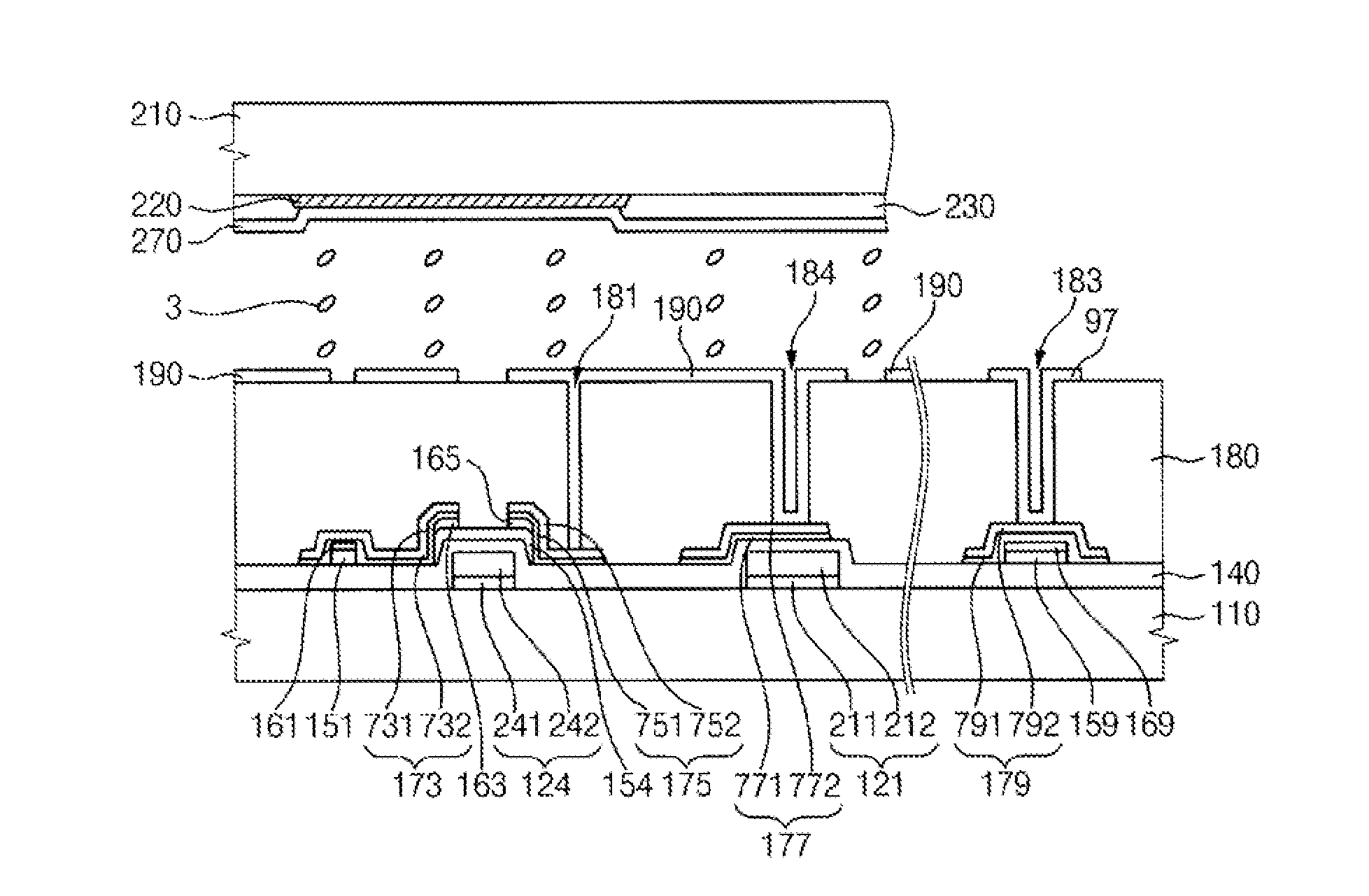
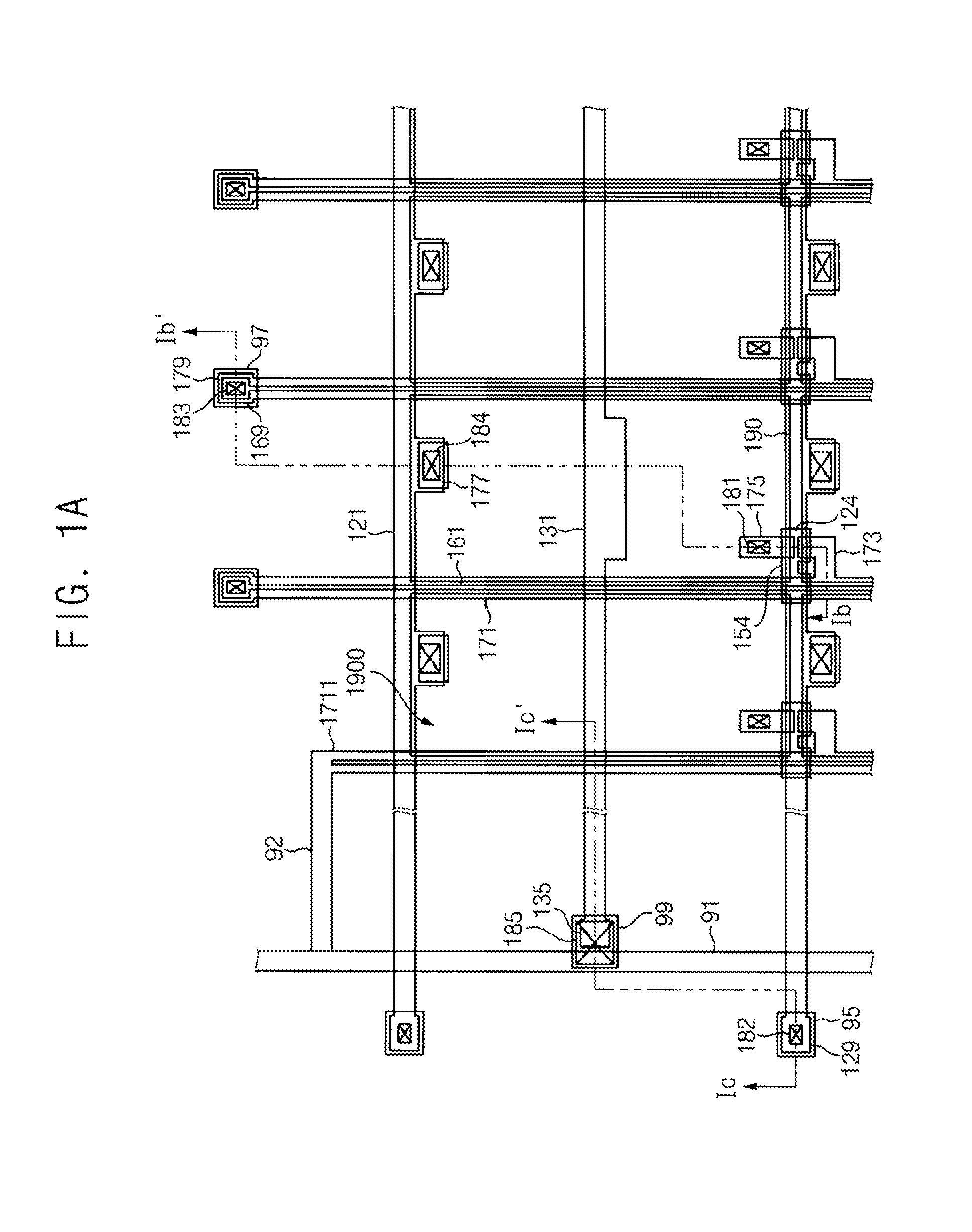
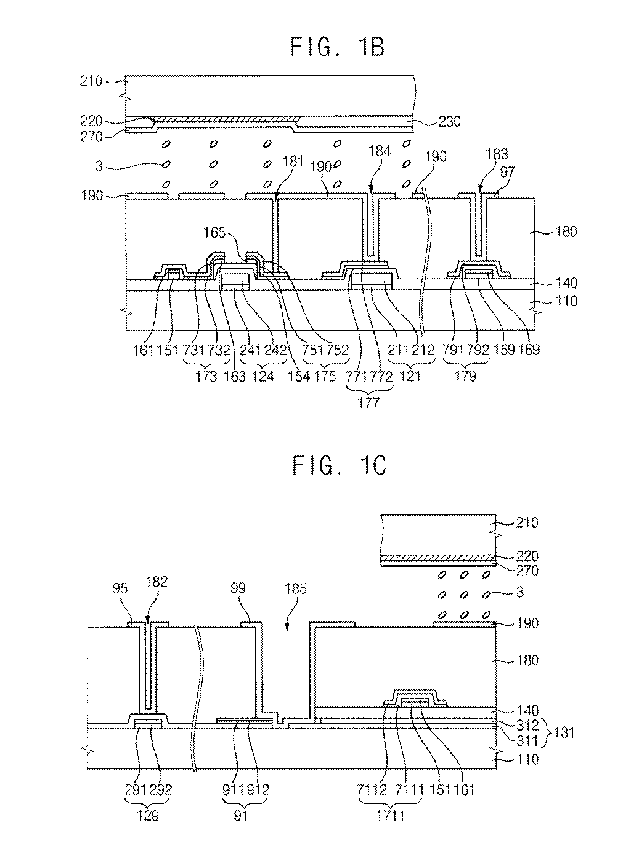
[0030]Exemplary embodiments of the present invention are described below with reference to the accompanying drawings. This invention may, however, be embodied in many different forms and should not be construed as limited to the exemplary embodiments set forth herein. In the drawings, the size and relative sizes of layers and regions may not be drawn to scale.

[0031]It will be understood that when an element or layer is referred to as being “on,”“connected to” or “coupled to” another element or layer, it can be directly on, connected or coupled to the other element or layer or intervening elements or layers may be present. Like numbers may refer to like elements throughout.

[0032]Hereinafter, exemplary embodiments of the present invention will be described with reference to the accompanying drawings.

[0033]FIG. 1A illustrates a portion of a display area of a TFT panel according to an exemplary embodiment. FIG. 1B is a cross-sectional view taken along the line Ib-Ib′ in FIG. 1. FIG. 1C ...


PUM


Abstract

A thin film transistor panel includes an insulating substrate including a display area and a peripheral area. A plurality of pixels is defined by a plurality of data lines that cross a plurality of gate lines. A pixel electrode is formed in each of the pixels. A plurality of dummy pixels is defined by a dummy data line that crosses the plurality of gate lines. A dummy pixel electrode is formed in each of the dummy pixels, and a thin film transistor including a gate electrode, a source electrode, a drain electrode, and a semiconductor. The thin film transistor display panel reduces or prevents a difference in brightness between pixels caused by a difference of coupling capacitance between the data line adjacent to the peripheral area and the other data lines.

Description

CROSS-REFERENCE TO RELATED APPLICATION[0001]This application claims priority to Korean Patent Application No. 10-2006-0088430, filed on Sep. 13, 2006, the contents of which are herein incorporated by reference in its entirety.BACKGROUND OF THE INVENTION[0002]1. Technical Field[0003]The present disclosure relates to a transistor panel and more particularly, to a thin film transistor panel and a liquid crystal display apparatus having the thin film transistor panel.[0004]2. Discussion of Related Art[0005]Generally, a liquid crystal display (LCD) apparatus includes a liquid crystal disposed between two substrates. An electric field provided between the two substrates changes an arrangement of liquid crystal molecules and controls the amount of light passing through the liquid crystal. The liquid crystal display apparatus displays an image by controlling the electric field and thereby controlling the passage of light through the liquid crystal. A thin film transistor (TFT) substrate, wh...

Claims


Application Information

Patent Timeline
IPC IPC(8): G06F3/038
CPCG02F1/1362G02F2001/133388G02F2001/13606G09G3/3611G09G2320/0233G09G2300/0413G09G2300/0426G09G2310/0232G09G2320/0209G09G3/3648G02F1/133388G02F1/13606G02F1/133
Inventor PARK, YONG-HANCHOI, JIN-YOUNGHER, YONG-KOOKWON, SUN-JA
Owner SAMSUNG ELECTRONICS CO LTD
Why Eureka
Try Eureka