Array substrate and display panel having the same

a display panel and substrate technology, applied in the field of array substrates and display panels, can solve problems such as the deterioration of the display quality of the lcd device, and achieve the effect of reducing the voltage variation of the pixel electrode and improving the display quality

a display panel and substrate technology, applied in the field of array substrates and display panels, can solve problems such as the deterioration of the display quality of the lcd device, and achieve the effect of reducing the voltage variation of the pixel electrode and improving the display quality

US20080100555A1Active Publication Date: 2008-05-01SAMSUNG DISPLAY CO LTD

Image

  • Array substrate and display panel having the same
  • Array substrate and display panel having the same
  • Array substrate and display panel having the same

Examples


Embodiment Construction

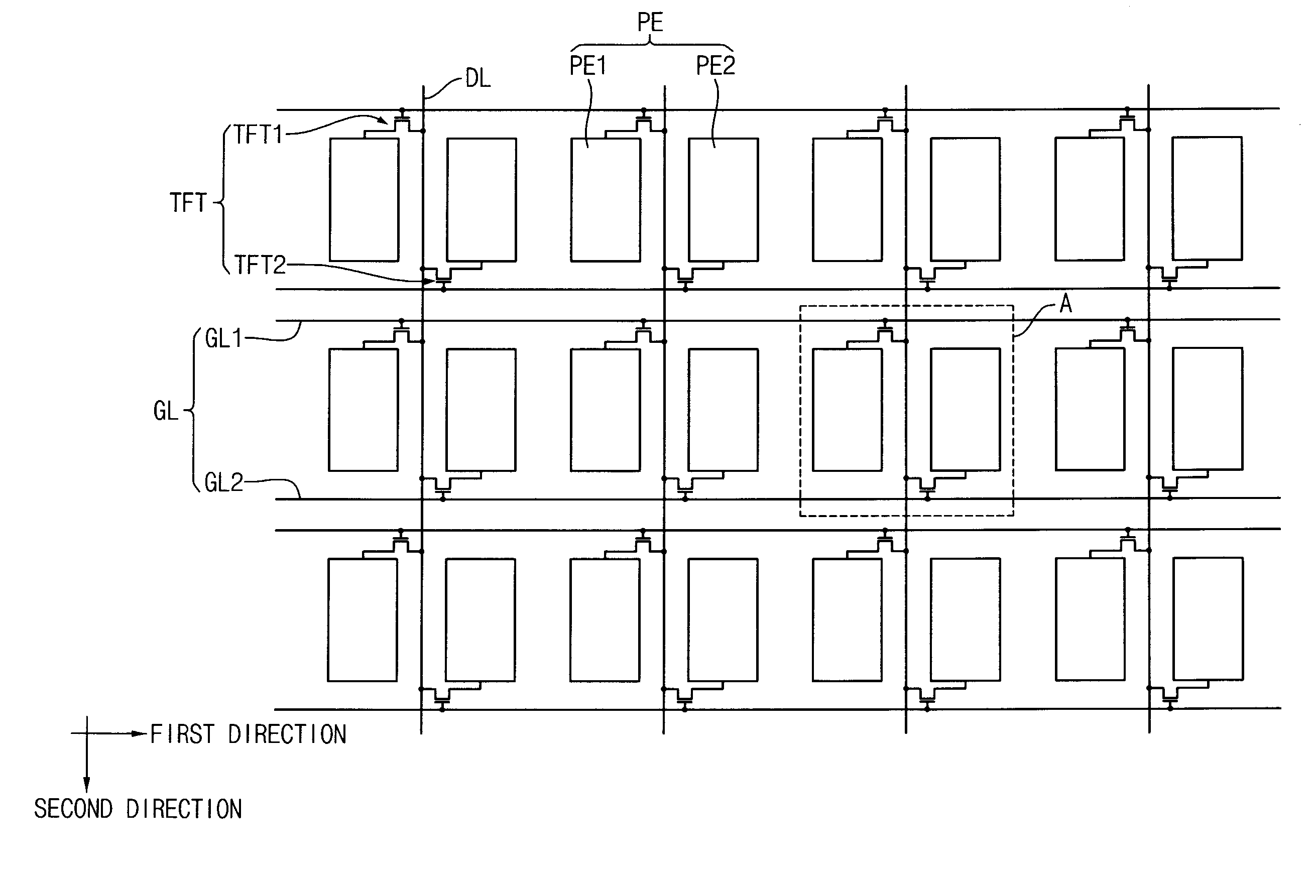
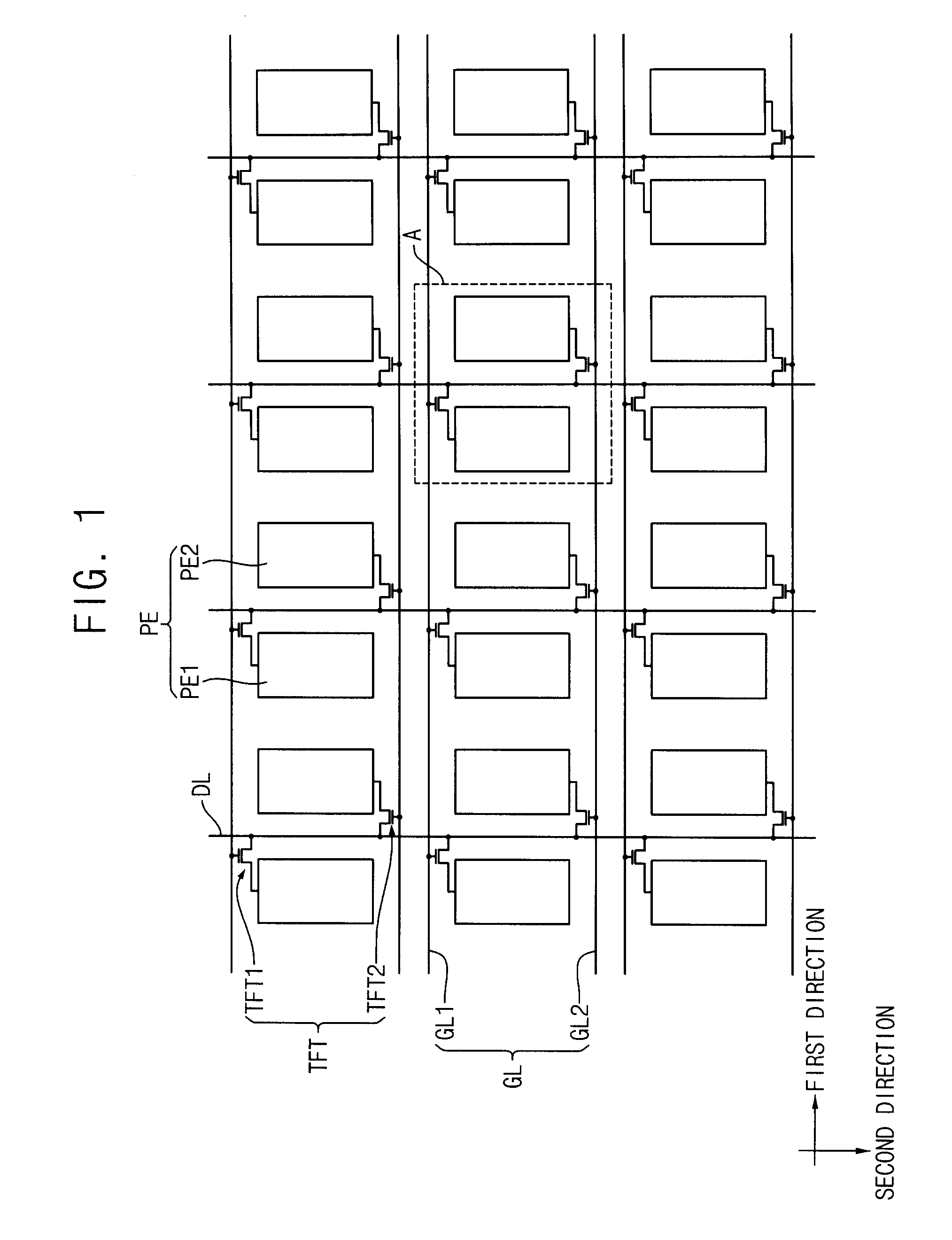
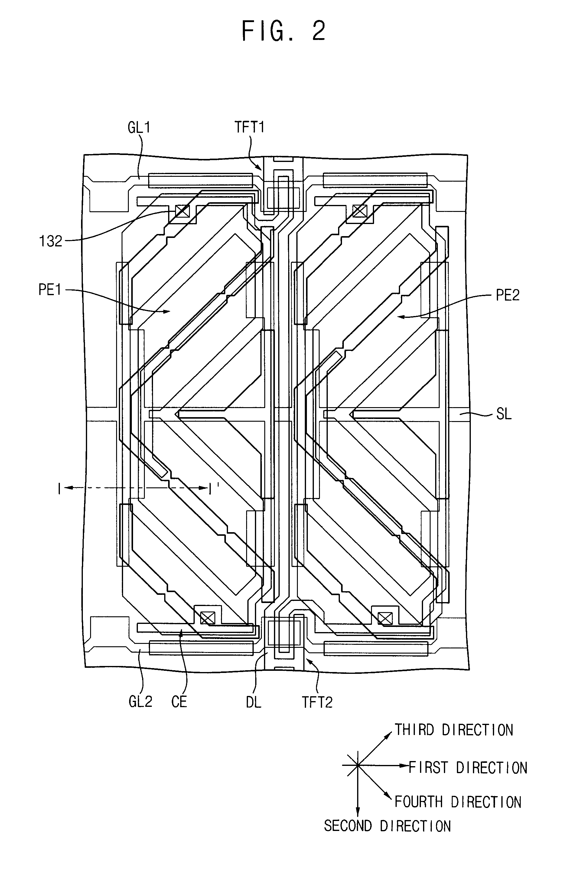
[0035]The invention is described more fully hereinafter with reference to the accompanying drawings, in which embodiments of the invention are shown. This invention may, however, be embodied in many different forms and should not be construed as limited to the embodiments set forth herein. Rather, these embodiments are provided so that this disclosure is thorough, and will fully convey the scope of the invention to those skilled in the art. In the drawings, the size and relative sizes of layers and regions may be exaggerated for clarity. Like reference numerals in the drawings denote like elements.

[0036]It will be understood that when an element or layer is referred to as being “on” or “connected to” another element or layer, it can be directly on or directly connected to the other element or layer, or intervening elements or layers may be present. In contrast, when an element is referred to as being “directly on” or “directly connected to” another element or layer, there are no int...


PUM


Abstract

An array substrate includes a gate line, a data line, a thin film transistor (TFT), a pixel electrode and a storage line. The pixel electrode includes a main pixel electrode and a sub pixel electrode partly surrounding at least a portion of the main pixel electrode. The storage line includes a main storage line that extends substantially parallel to the gate line and across the pixel electrode, a sub storage line that extends from the main storage line and substantially parallel to the data line to overlap the sub pixel electrode, and a protruding storage line that extends from the sub storage line and substantially parallel to the gate line to overlap the main pixel electrode.

Description

CROSS-REFERENCE TO RELATED APPLICATIONS[0001]This application claims priority from and the benefit of Korean Patent Application No. 10-2006-0107006, filed on Nov. 1, 2006, which is hereby incorporated by reference for all purposes as if fully set forth herein.BACKGROUND OF THE INVENTION[0002]1. Field of the Invention[0003]The present invention relates to an array substrate and a display panel including the same. More particularly, the present invention relates to an array substrate that may be capable of improving display quality and a display panel including the same.[0004]2. Discussion of the Background[0005]A liquid crystal display (LCD) device as a flat panel display device includes an LCD panel displaying an image by using optical characteristics of the liquid crystal and a backlight assembly disposed under the LCD panel to provide light to the LCD panel.[0006]The LCD panel includes an array substrate, a color filter substrate facing the array substrate, and a liquid crystal la...

Claims


Application Information

Patent Timeline
01 May 2008
Publication
US20080100555A1
IPC
G09G3/36
CPC
G02F1/134336; G02F2001/134345; G02F1/13624; G02F1/136213; G02F1/134345; G02F1/1343
Inventors
YOON, YEO GEON; LEE, WON-HEE