
Preparation method for electronic components with an alloy electrode layer

a technology of alloy electrode and electronic components, which is applied in the direction of non-metallic protective coating application, printed element electric connection formation, conductive pattern formation, etc., can solve the problems of inability to guarantee the acceptance rate of mass-produced varistors, the copper electrode of varistor fabricated by the conventional technique is prone to oxidation, and the conventional technique is not so cost-effective. achieve the effect of enhancing the reliability of base metal copper electrod

Inactive Publication Date: 2016-10-06
THINKING ELECTRONICS INDAL
View PDF5 Cites 1 Cited by
  • Summary
  • Abstract
  • Description
  • Claims
  • Application Information

AI Technical Summary

Benefits of technology

This patent is about a new way to make electronic components with a copper alloy electrode layer. This layer is integrated into a multilayer structure, which helps to improve the reliability of the component in high-temperature environments. The use of this copper alloy layer also helps to reduce the cost of the component. The resulting component has a lower voltage variation and can withstand more waves of electricity before failing.

Problems solved by technology

However, the copper electrode of the varistor fabricated by the conventional technique is prone to oxidation under high-temperature operation, which becomes a durability issue for electronic appliances at home or in industrial area.
Additionally, as such conventional technique also needs to consume lots of inert gas, despite the cost down effect arising from the base metal, the varistor produced by the conventional technique is not so cost-effective because of the rising auxiliary production costs.
Due to the tendency of oxygen absorption, acceptance rate of mass-produced varistors cannot be guaranteed.

Method used

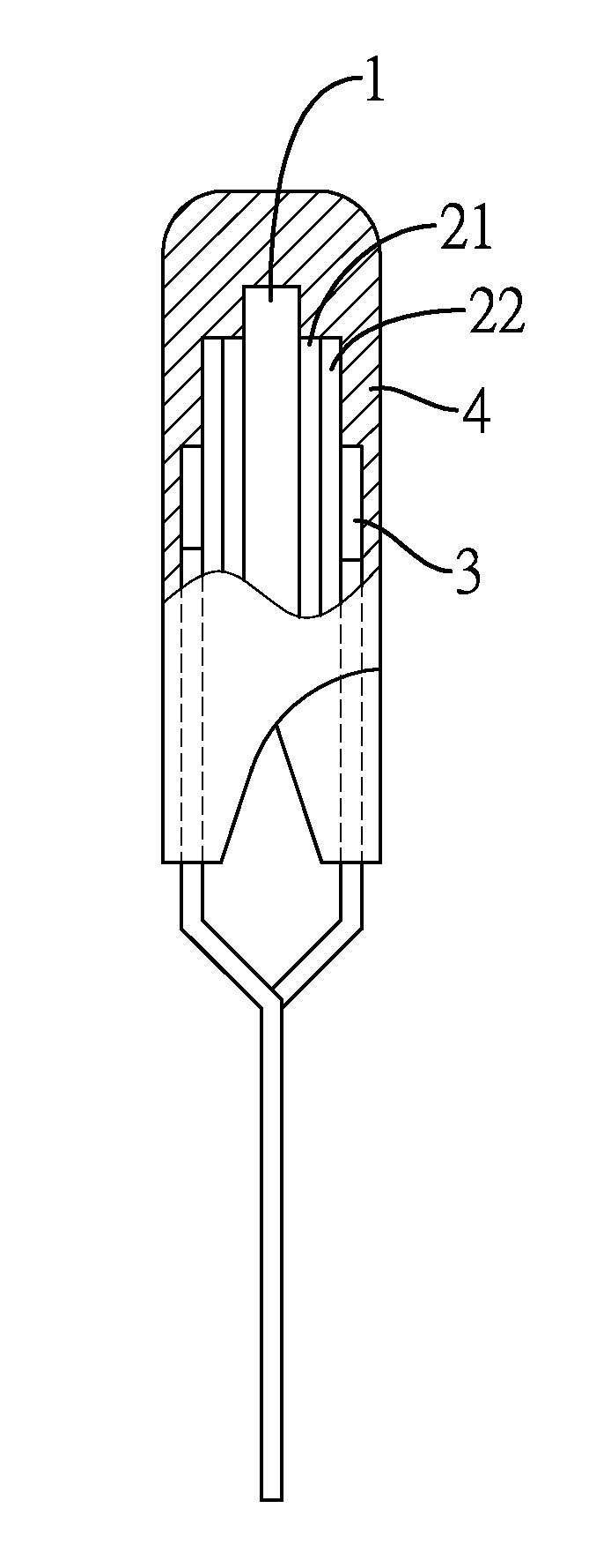
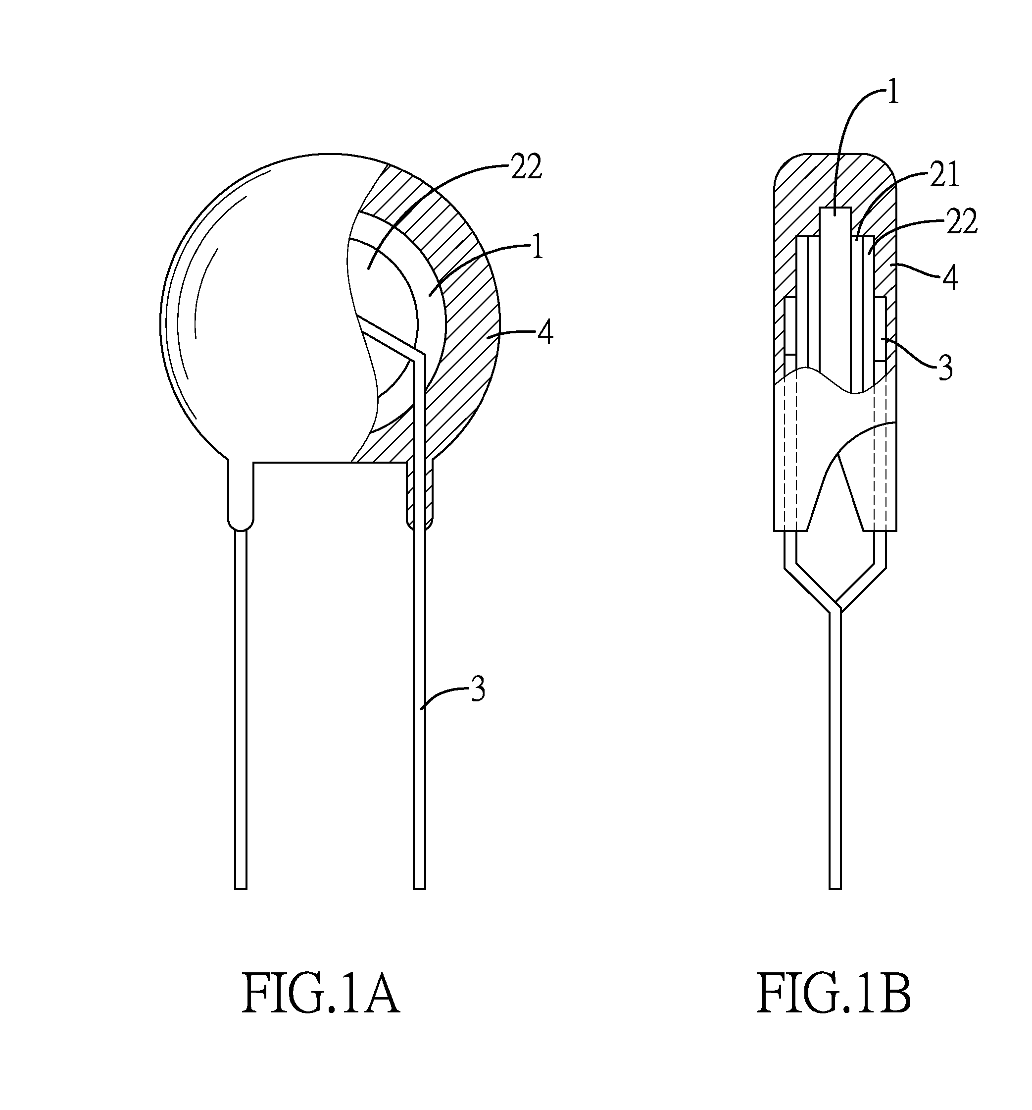
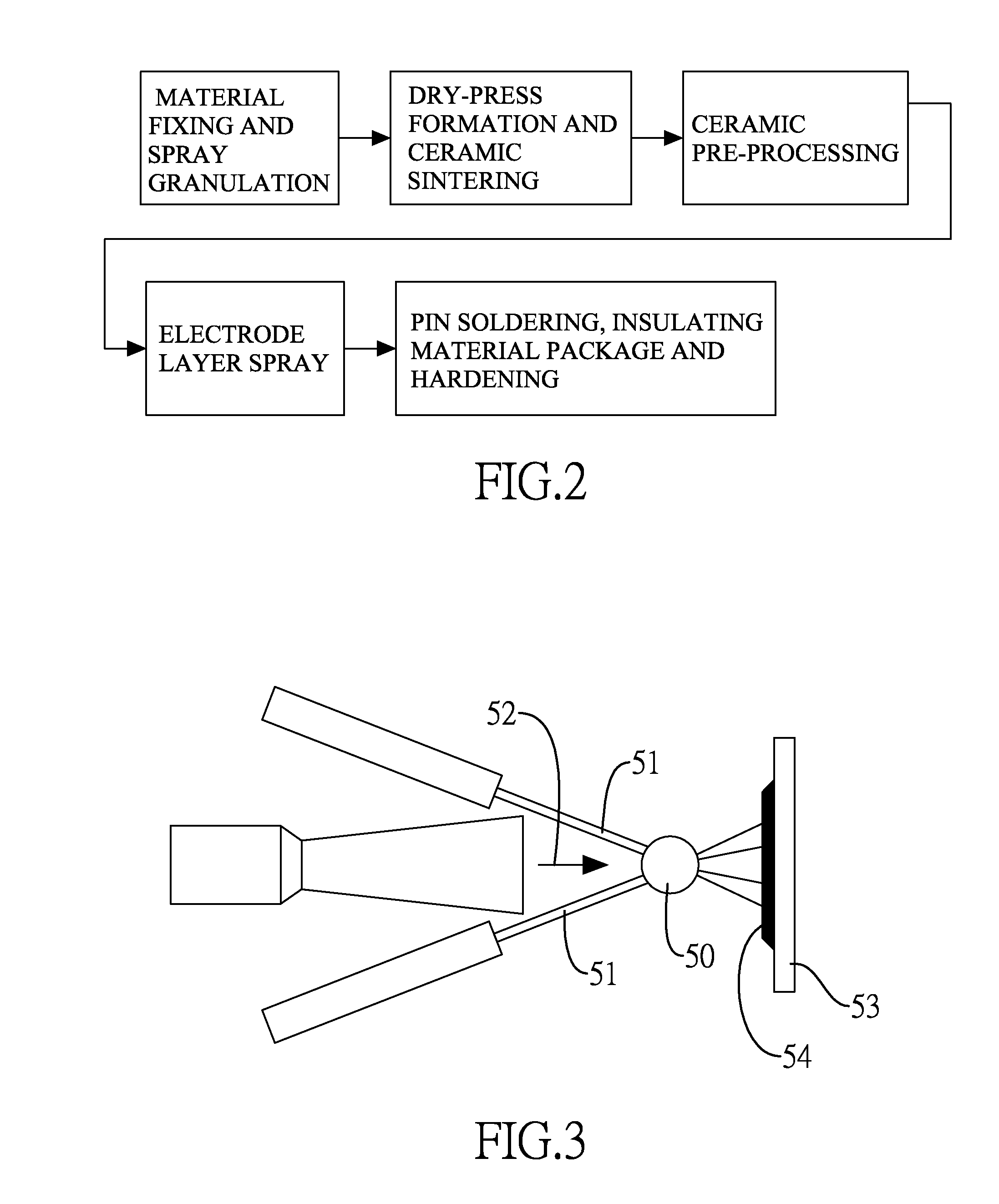

Image

  • Preparation method for electronic components with an alloy electrode layer
  • Preparation method for electronic components with an alloy electrode layer
  • Preparation method for electronic components with an alloy electrode layer

Examples


first embodiment

[0024]Steps of producing the metal layers 21:

[0025]1. Clean surfaces of the ceramic substrate 1.

[0026]2. Blend glass powder and a binder with pure aluminum powder to acquire an aluminum slurry with a weight percent of aluminum in a range of 65˜75%. The glass powder includes silicon dioxide (SiO2), bismuth oxide (BiO2) and boron trioxide (B2O3) and has a weight percent in a range of 10%˜15%. The binder has a weight percent in a range of 10%˜25% and the contents of the binder include ethylcellulose and terpineol. The aluminum slurry can be coated on a first surface of the ceramic substrate 1 through silk-screen printing.

[0027]3. Place the ceramic substrate 1 printed with the aluminum slurry into an oven for baking for 60 minutes at 100° C., remove the ceramic substrate 1 done with the baking, coat the aluminum slurry on a second surface opposite to the first surface through the same silk-screen printing, and place the ceramic substrate 1 back into the oven and bake for 60 minutes at 1...


PUM


Abstract

A preparation method for an electronic component with an alloy electrode layer includes steps of printing a metal layer on each of the two opposite surfaces of a ceramic substrate with the metal layer made from aluminum, spraying an alloy layer being a copper alloy layer on an outer surface of each metal layer, connecting a pin to each alloy layer, and enclosing the ceramic substrate, the metal layers, the alloy layers and a portion of each pin with an insulating layer. With the adoption of copper alloy for the alloy layer, the preparation method has the advantages of low production cost and high reliability of the electronic component produced by the method.

Description

BACKGROUND OF THE INVENTION[0001]1. Field of the Invention[0002]The present invention relates to a preparation method for an electronic component and, more particularly, to a preparation method for an electronic component with an alloy electrode layer.[0003]2. Description of the Related Art[0004]Varistor is a delicate electronic ceramic component that is fabricated from a mixture of a base material, which includes electronic grade zinc oxide (ZnO) powder, and various small amount of additives, such as electronic grade bismuth oxide (Bi2O3), cobalt oxide (Co2O3), manganese dioxide (MnO2), antimony trioxide (Sb2O3), titanium dioxide (TiO2), chromium oxide (Cr2O3), nickel oxide (Ni2O3) and the like added thereto, through mixing, molding and sintering processes, making that the varistor is naturally sensitive to variation of externally applied voltage and it is thus applicable for the varistor to sense and limit all transient overvoltage occurring in circuit and absorb the resulting sur...

Claims


Application Information

Patent Timeline
IPC IPC(8): H01C17/065H05K3/28H05K3/40H05K3/46H05K3/12H05K3/14
CPCH01C17/065H05K3/1225H05K3/14H05K3/1291H05K3/4664H05K3/28H05K3/4007H01C1/142H01C7/102H01C17/281H01C17/283
Inventor XU, XUNJIA, ZHIWEI
Owner THINKING ELECTRONICS INDAL
Learn More